RFID chip impedance measurement method and device based on two-port network

An impedance measurement and two-port technology, which is applied in the field of RFID chip impedance measurement methods and devices, can solve the problems of high personnel requirements, complex algorithms, and inaccurate results, and achieve low personnel requirements, simple algorithms, and accurate measurement results.

Active Publication Date: 2019-03-08
BEIJING CHIP IDENTIFICATION TECH CO LTD +2
View PDF6 Cites 7 Cited by
  • Summary
  • Abstract
  • Description
  • Claims
  • Application Information

AI Technical Summary

Problems solved by technology

The problem of the prior art is: in the first single-port network de-embedding method, the test port is asymmetrical, while the chip port is symmetrical. When the asymmetrical port is directly connected to the symmetrical port, it involves balanced-unbalanced conversion. resulting in inaccurate results
The second TRL de-embedding method needs to make four calibration circuit boards. When using the four sets of S parameters tested for error correction, the algorithm itself is too complicated and requires too much personnel

Method used


Image

  • RFID chip impedance measurement method and device based on two-port network
  • RFID chip impedance measurement method and device based on two-port network
  • RFID chip impedance measurement method and device based on two-port network

Examples


Embodiment Construction

[0032] The specific embodiments of the present invention will be described in detail below in conjunction with the accompanying drawings, but it should be understood that the protection scope of the present invention is not limited by the specific embodiments.

[0033] Unless expressly stated otherwise, throughout the specification and claims, the term "comprise" or variations thereof such as "includes" or "includes" and the like will be understood to include the stated elements or constituents, and not Other elements or other components are not excluded.

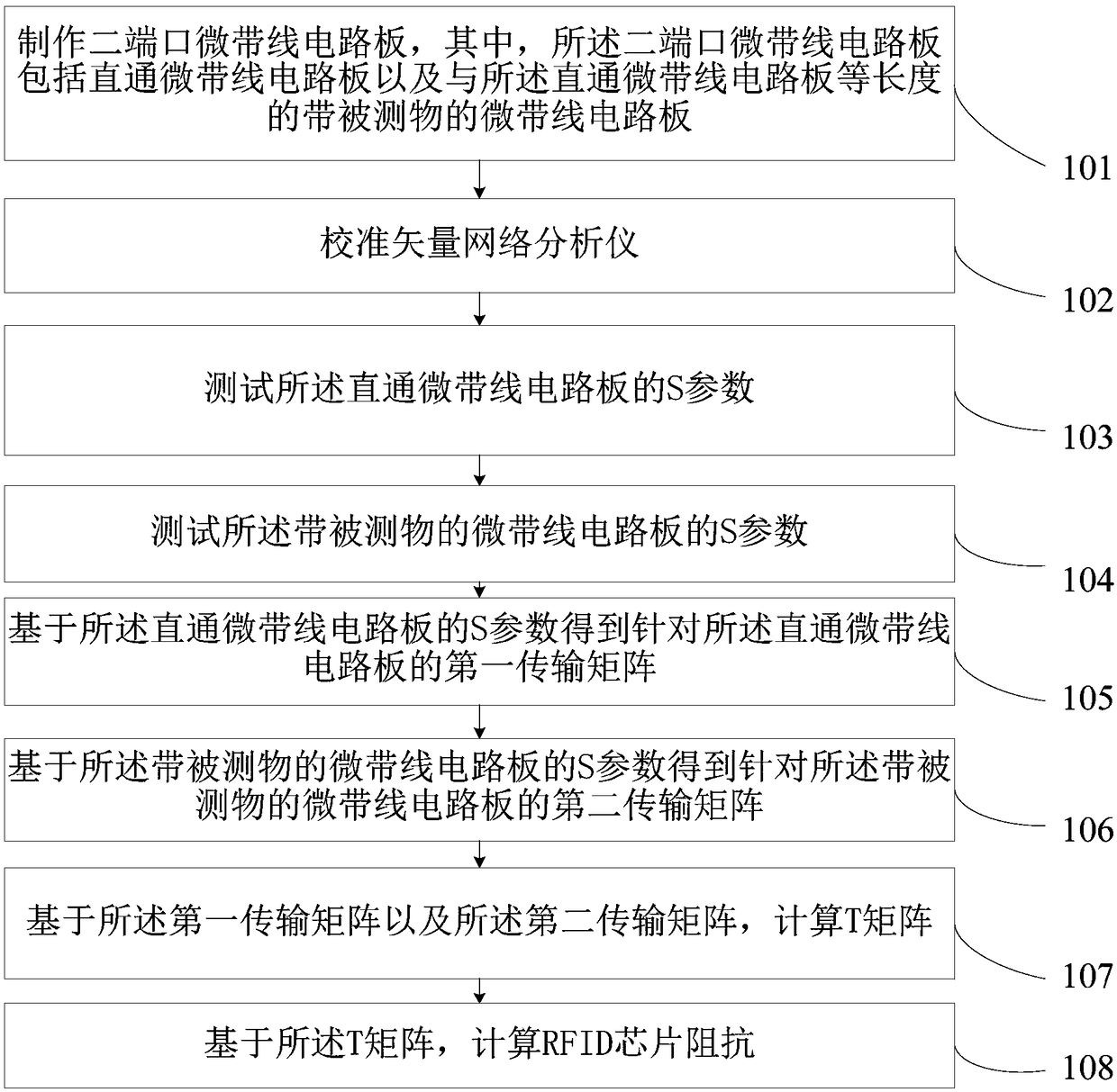
[0034] Such as figure 1 Shown, the RFID chip impedance measuring method based on two-port network of preferred embodiment of the present invention comprises the steps:

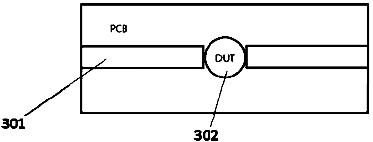
[0035] Step 101: Fabricate a two-port microstrip line circuit board, wherein the two-port microstrip line circuit board includes a straight-through microstrip line circuit board and a microstrip with an object under test having the same length as the throu...


PUM


Abstract

The invention discloses an RFID chip impedance measurement method and device based on a two-port network. The RFID chip impedance measurement method comprises the following steps of making a two-portmicrostrip line circuit board, wherein the two-port microstrip line circuit board includes a straight through microstrip line circuit board and a microstrip line circuit board with a tested object having the same length with the straight through microstrip line circuit board; calibrating a vector network analyzer; testing the S parameter of the straight through microstrip line circuit board; testing the S parameter of the microstrip line circuit board with the tested object; acquiring a first transmission matrix aiming at the straight through microstrip line circuit board based on the S parameter of the straight through microstrip line circuit board; acquiring a second transmission matrix aiming at the microstrip line circuit board with the tested object based on the S parameter of the microstrip line circuit board with the tested object; based on the first transmission matrix and the second transmission matrix, calculating a T matrix; and based on the T matrix, calculating an RFID chip impedance. By using the RFID chip impedance measurement method, a measurement result is accurate and an algorithm is simple.

Description

technical field [0001] The invention belongs to the technical field of wireless communication, and relates to a method and a device for measuring the impedance of an RFID chip based on a two-port network. Background technique [0002] The farthest reading and writing distance can be achieved when the RFID chip and antenna impedance are conjugate matched. Therefore, it is necessary to measure the chip impedance before designing the antenna, and then design the antenna impedance according to the measurement result. There are usually two methods to test chip impedance, the first is the single-port network de-embedding method, and the second is the TRL de-embedding method. The first is the single-port network de-embedding method. First, the S parameters of the test board are obtained. After obtaining the overall S parameters, matrix operations are used to remove the S parameters of the test board. This test algorithm can be performed using the classic microwave network S paramet...

Claims


Application Information

Patent Timeline
Patent Type & Authority Applications(China)
IPC IPC(8): G01R27/02
CPCG01R27/02
Inventor 刘科煜杜鹏程陈会军李杰伟李建强张海峰唐晓柯
Owner BEIJING CHIP IDENTIFICATION TECH CO LTD
Why Eureka
Try Eureka