Size detecting mechanism for producing silicon wafers

A size detection and silicon wafer technology, applied in the field of size detection mechanism for silicon wafer production, can solve the problems of high error rate of manual detection, difficulty in fixing silicon wafer, low efficiency of manual detection, etc., and achieve simple operation, high detection accuracy, The effect of efficient detection

Inactive Publication Date: 2019-03-12
西安科技成果转化工程有限公司
View PDF0 Cites 6 Cited by
  • Summary
  • Abstract
  • Description
  • Claims
  • Application Information

AI Technical Summary

Problems solved by technology

[0004] In order to solve the above problems, the present invention provides a size detection mechanism for silicon wafer production, which can solve the difficulties in fixing the silicon wafer when manually detecting the size of the silicon wafer, the low efficiency of manual detection, and the need to recalculate whether the size is within the allowable error range High error rate of internal and manual detection and easy confusion between qualified products and unqualified products can realize efficient detection of silicon wafer size, with simple operation, high detection accuracy, high detection efficiency and convenient distinction between qualified products and unqualified products Etc

Method used


Image

  • Size detecting mechanism for producing silicon wafers
  • Size detecting mechanism for producing silicon wafers
  • Size detecting mechanism for producing silicon wafers

Examples


Embodiment Construction

[0021] In order to make the technical means, creative features, goals and effects achieved by the present invention easy to understand, the present invention will be further described below in conjunction with specific illustrations. It should be noted that, in the case of no conflict, the embodiments in the present application and the features in the embodiments can be combined with each other.

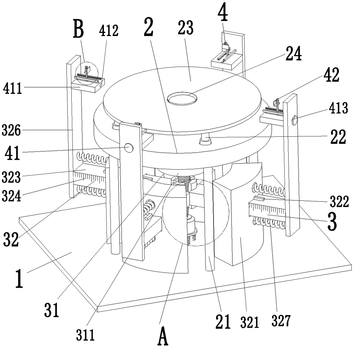
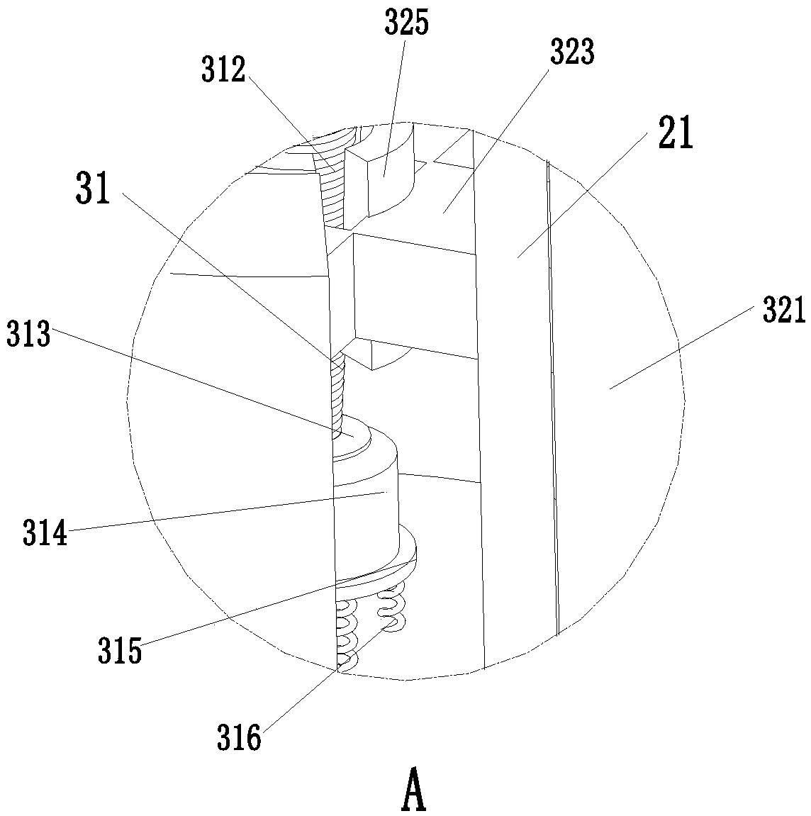
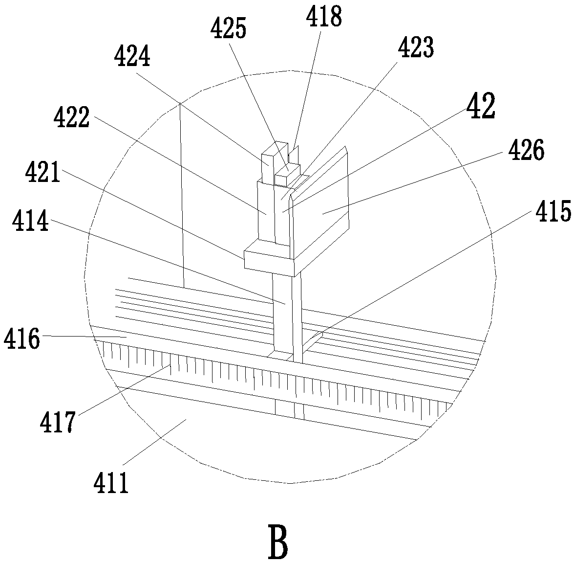
[0022] Such as Figure 1 to Figure 3 As shown, a size detection mechanism for silicon wafer production includes a base plate 1, a detection platform 2, an adjustment mechanism 3 and an alarm mechanism 4. A detection platform 2 is installed in the middle of the upper end surface of the bottom plate 1, and the distance between the detection platform 2 and the base plate 1 is An adjustment mechanism 3 is installed between them, and an alarm mechanism 4 is installed on the right side of the adjustment mechanism 3.

[0023] The upper end of the base plate 1 is equipped with a detection p...


PUM


Abstract

The invention relates to a size detecting mechanism for producing silicon wafers. The size detecting mechanism for producing silicon wafers includes a bottom plate, a detection table, an adjustment mechanism and an alarm mechanism, wherein the detection table is arranged in the middle portion of the upper end surface of the bottom plate; the adjustment mechanism is arranged between the detection table and the bottom plate; the alarm mechanism is arranged on the right side of the adjustment mechanism; the detection table is arranged on the upper end of the bottom plate; and the upper end surface of the detection table is uniformly provided with electric detection push columns in the circumferential direction of the detection table. According to the size detecting mechanism, the problems that when the sizes of the silicon wafers are detected manually, the silicon wafers are difficult to fix; the manual detection efficiency is low; the sizes need re-calculation whether the sizes are within the allowable error range; the manual detection error rate is high; and qualified unqualified products are easily confused are solved; the high-efficiency detection of the silicon wafer sizes can berealized; and the size detecting mechanism has the advantages of simple operation, high detection accuracy, high detection efficiency, and convenient distinction between qualified and unqualified products.

Description

technical field [0001] The invention relates to the field of silicon wafer processing, in particular to a size detection mechanism for silicon wafer production. Background technique [0002] With the continuous advancement of science and technology, the production technology of silicon wafers is becoming more and more mature. Silicon wafers have been widely used in the fields of chips, electronics, batteries, etc. The processing of silicon wafers generally goes through sticking, prescription, glue removal, In the steps of rolling, slicing, cleaning and drying, testing, and packaging, some processes in the entire production line are mechanically operated, but some processes are manually operated, and the two steps of degumming and testing are mainly manual. [0003] During the detection process of silicon wafer processing, the size of the silicon wafer is detected by manually placing the silicon wafer on the granite measuring instrument. The manual inspection has complex fixi...

Claims


Application Information

Patent Timeline
IPC IPC(8): B07C5/02B07C5/06B07C5/36
CPCB07C5/02B07C5/06B07C5/36
Inventor 赵续凯
Owner 西安科技成果转化工程有限公司
Why Eureka
Try Eureka