Gate driving circuit and display device thereof

A gate drive circuit and gate drive technology, applied in static indicators, instruments, etc., can solve the problems of display device bad risk, frame increase, height reduction, etc., to reduce the probability of bad risk and integration difficulty , the effect of saving manufacturing costs

Active Publication Date: 2019-03-12
KUSN INFOVISION OPTOELECTRONICS
View PDF10 Cites 5 Cited by
  • Summary
  • Abstract
  • Description
  • Claims
  • Application Information

AI Technical Summary

Problems solved by technology

[0003] In the prior art, one gate drive unit drives one scan line. When the resolution of the display panel is higher, the number of gate drive units increases so that the height of the gate drive circuit structure decreases and the width increases accordingly, so that the frame also correspondingly The increase of the display device makes it more difficult to realize the narrow bezel
And the increase in the number of gate drive units will cause the display device to have a bad risk

Method used


Image

  • Gate driving circuit and display device thereof
  • Gate driving circuit and display device thereof
  • Gate driving circuit and display device thereof

Examples


Embodiment Construction

[0027] Hereinafter, the present invention will be described in more detail with reference to the accompanying drawings. In the various drawings, like elements are indicated with like reference numerals. For the sake of clarity, various parts in the drawings have not been drawn to scale. Also, some well-known parts may not be shown in the drawings.

[0028] In the following, many specific details of the present invention are described, such as structures, materials, dimensions, processes and techniques of components, for a clearer understanding of the present invention. However, the present invention may be practiced without these specific details, as will be understood by those skilled in the art.

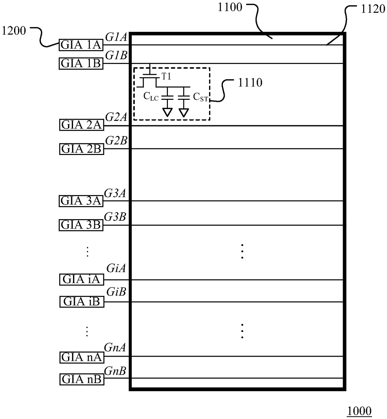
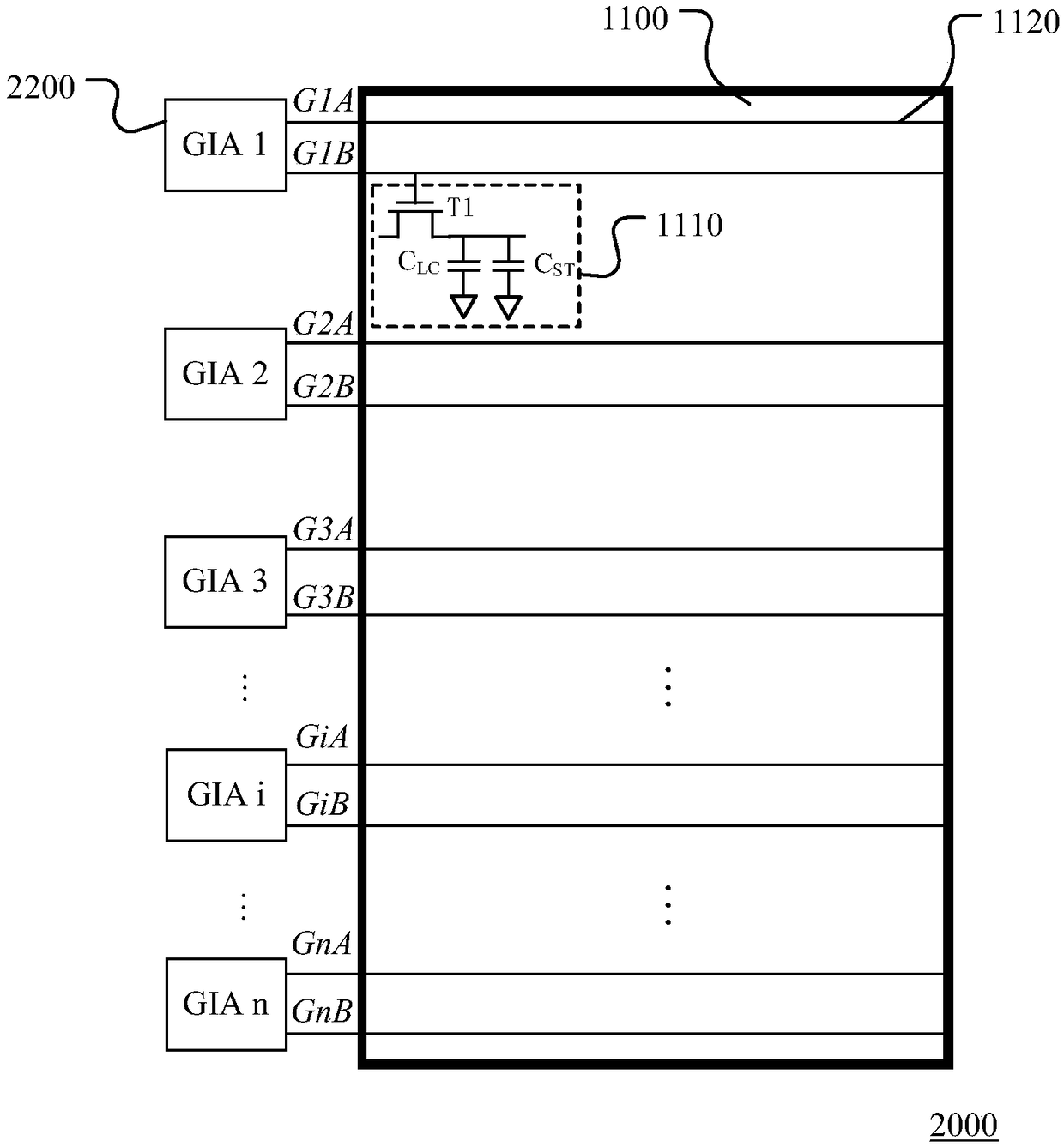
[0029] figure 2 A schematic structural view showing a display device according to the present invention, such as figure 2 As shown, the display device 2000 provided by the embodiment of the present invention includes a display panel 1100 and a gate driving circuit, wherein th...


PUM


Abstract

The invention discloses a gate driving circuit and a display device thereof. The gate driving circuit comprises multi-stage gate driving units, wherein each gate driving unit comprises an input module, an output module and a drop module, wherein each input module is used for conducting precharging according to a pre-stage driving signal and supplying voltage to first and second nodes; each outputmodule generates a first gate driving signal according to a first clock signal and the voltage of the first nodes and generates a second gate driving signal according to a second clock signal and thevoltage of the second nodes; each drop module generates a first drop signal to drop the voltage of the first nodes according to a third clock signal and generates a second drop signal to drop the voltage of the second nodes according to a subsequent driving signal, and the first gate driving signals and the second gate driving signals sequentially drive two adjacent gate lines on a display panel.According to the gate driving circuit and the display device thereof, on the basis of high resolution, the number of the gate driving units is reduced by half, so that the probability that the displaydevice may be attacked by an adverse risk is reduced, and the narrow-frame design of the display device with high resolution is facilitated.

Description

technical field [0001] The present invention relates to the field of display technology, and more particularly relates to a gate drive circuit and a display device thereof. Background technique [0002] figure 1 A schematic diagram showing the structure of a display device in the prior art, such as figure 1 As shown, the display device 1000 includes a display panel 1100, a gate driving circuit and a source driving circuit (not shown in the figure). The gate drive circuit includes 2n levels of GIA (Gate Driver in Array, integrated gate drive circuit) units 1200, where n is a non-zero natural number. The display panel 1100 includes a plurality of pixel units 1110 arranged in an array and 2n scanning lines 1120 for transmitting gate driving signals, and each pixel unit includes a thin film transistor T1, a liquid crystal capacitor C LC and storage capacitor C ST . In the display panel 1100, the gates of the thin film transistors in the pixel units 1110 in the same row are ...

Claims


Application Information

Patent Timeline
Patent Type & Authority Applications(China)
IPC IPC(8): G09G3/20
CPCG09G3/20G09G2310/0267
Inventor 李海波郑会龙邹忠飞陈尧
Owner KUSN INFOVISION OPTOELECTRONICS
Why Eureka
Try Eureka