

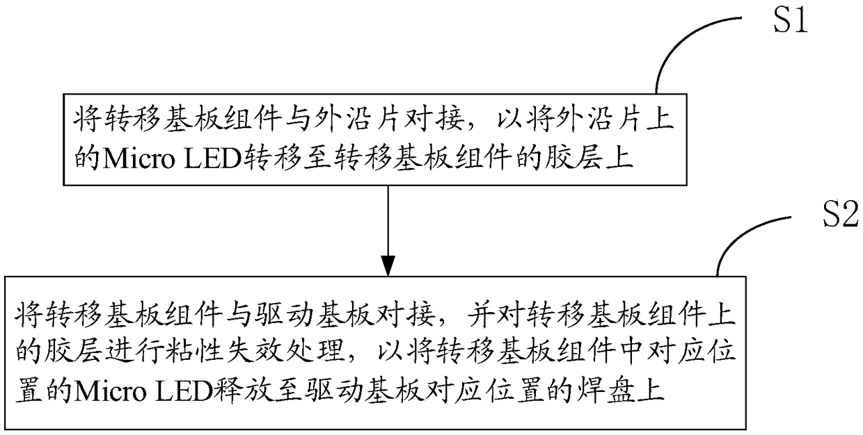
Manufacture method for Micro LED (Light Emitting Diode) display substrate
A manufacturing method and display substrate technology, applied in semiconductor/solid-state device manufacturing, electrical components, electrical solid-state devices, etc.
- Summary
- Abstract
- Description
- Claims
- Application Information
AI Technical Summary
Problems solved by technology
Method used
Image

Examples
Embodiment 1
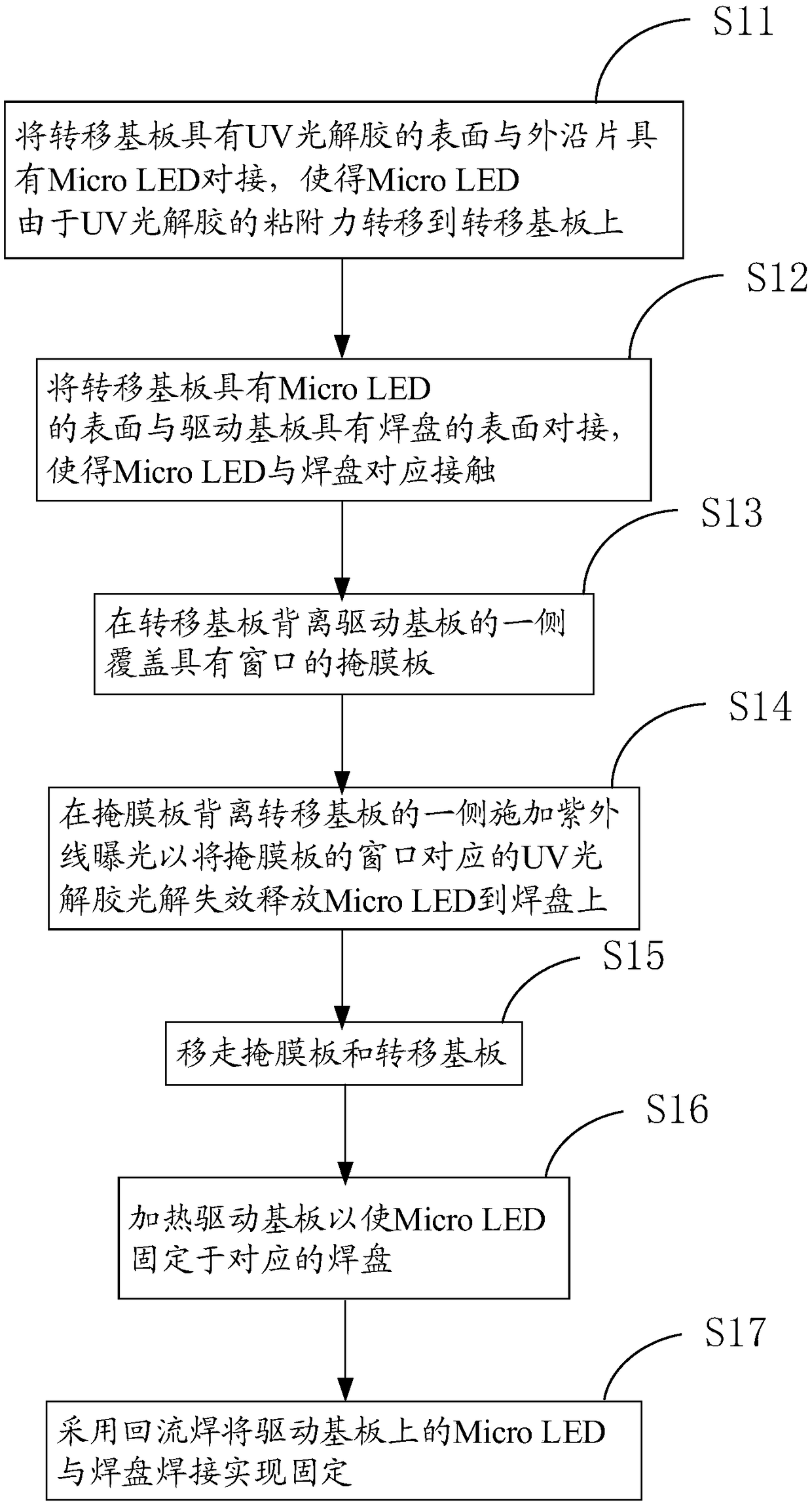
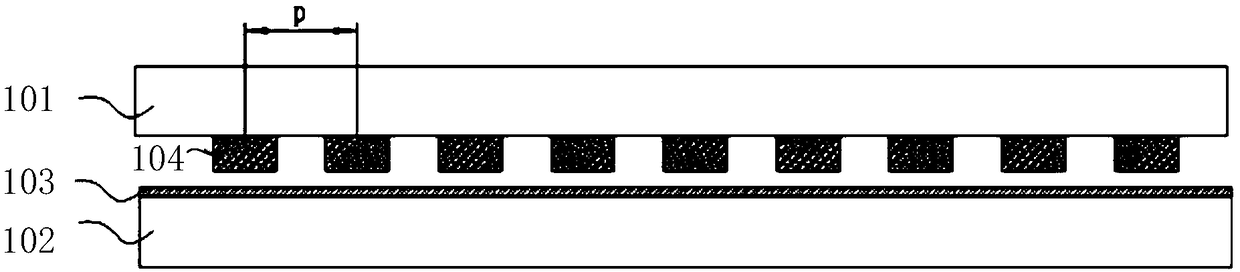
[0048] refer to Figure 2 to Figure 11In the manufacturing method of the Micro LED104 display substrate provided in this embodiment, the transfer substrate assembly includes a transfer substrate 102, and the glue layer used to adhere the Micro LED104 to the transfer substrate 102 is UV photolytic glue 103, such as figure 2 As shown, the production method includes the following steps:
[0049] Step S11, refer to image 3 , docking the surface of the transfer substrate 102 with the UV photolytic glue 103 and the outer edge sheet 101 with the Micro LED 104, so that the Micro LED 104 is transferred to the transfer substrate 102 due to the adhesion of the UV photolytic glue 103, Figure 4 It is shown that the Micro LED 104 has been transferred onto the UV photoresist 103 of the transfer substrate 102 .
[0050] Wherein, the transfer substrate 102 is made of a transparent material, and a layer of the above-mentioned UV photoresist 103 is coated on the surface of the transfer subs...
Embodiment 2
[0069] refer to Figure 12 to Figure 19 , in the manufacturing method of the Micro LED104 display substrate provided in this embodiment, the transfer substrate assembly includes an auxiliary transfer substrate 105 and a transfer substrate 102, the auxiliary transfer substrate 105 has an organic glue 106, and the transfer substrate 102 has a UV curable glue 107. The method first transfers the Micro LED 104 on the outer edge sheet 101 to the auxiliary transfer substrate 105, and then transfers the Micro LED 104 on the auxiliary transfer substrate 105 to the driving substrate 301, as Figure 12 As shown, it specifically includes the following steps:
[0070] Step S21, refer to Figure 13 , the auxiliary transfer substrate 105 is docked with the outer edge sheet 101 to adhere the Micro LED 104 on the outer edge sheet 101 to the organic glue 106 .
[0071] After the auxiliary transfer substrate 105 is docked with the outer edge sheet 101, the Micro LED 104 on the outer edge sheet...
PUM
 Abstract
Description
Claims
Application Information