Method for manufacturing buried-inductor printed circuit board

A technology of printed circuit board and manufacturing method, which is applied in the directions of printed circuit manufacturing, assembling printed circuits with electrical components, printed circuits, etc., can solve the problems of affecting the electrical performance of metallized holes, small inductance value, and unrealistic glue filling, etc. To solve the problem of insufficient surface installation space, improve packaging efficiency, and avoid cumbersome effects

Active Publication Date: 2019-03-19
XIAN MICROELECTRONICS TECH INST
View PDF3 Cites 0 Cited by
  • Summary
  • Abstract
  • Description
  • Claims
  • Application Information

AI Technical Summary

Problems solved by technology

[0004] Compared with the traditional printed circuit board processing method, the horizontal and vertical buried induction coil method can complete the inductance function without magnetic materials and the method is simple, but the inductance value is small, generally hundreds of nanohenries to several thousand nanohenries; Using the method of embedding the inductor coil with magnetic materials to directly embed the magnetic core into the printed board, there may be false glue filling, resulting in air bubbles in the resin around the printed board coil, which will affect the electrical performance of the subsequent metallized holes

Method used


Image

  • Method for manufacturing buried-inductor printed circuit board
  • Method for manufacturing buried-inductor printed circuit board
  • Method for manufacturing buried-inductor printed circuit board

Examples


Embodiment Construction

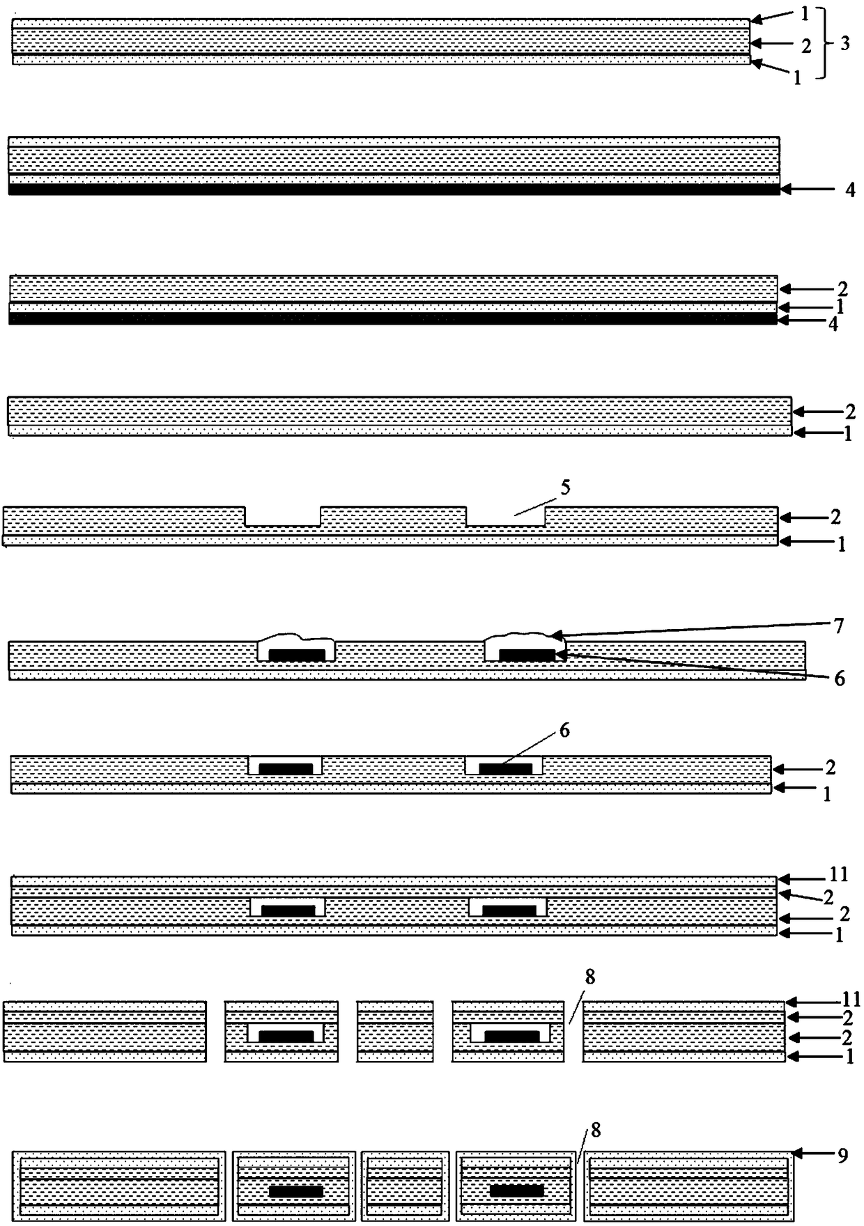
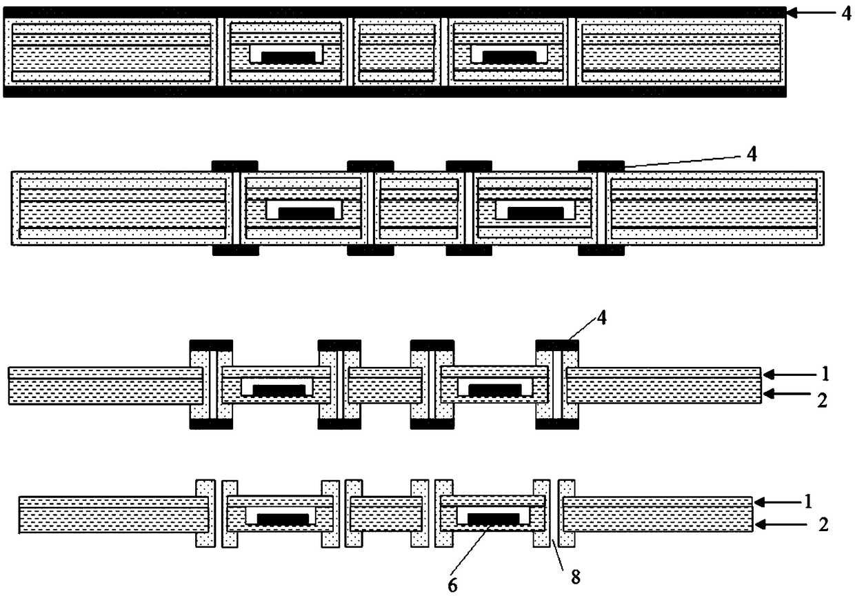
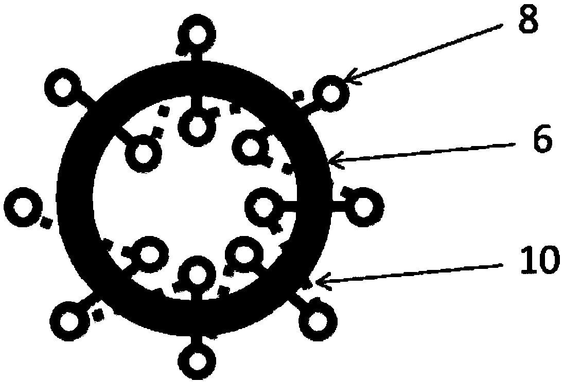
[0046] The present invention will be described in detail below in conjunction with the accompanying drawings and specific embodiments.

[0047] In describing the present invention, it should be understood that the terms "center", "longitudinal", "transverse", "upper", "lower", "front", "rear", "left", "right", " The orientations or positional relationships indicated by "vertical", "horizontal", "top", "bottom", "inner" and "outer" are based on the orientations or positional relationships shown in the drawings, and are only for the convenience of describing the present invention and Simplified descriptions, rather than indicating or implying that the device or element referred to must have a particular orientation, be constructed and operate in a particular orientation, and thus should not be construed as limiting the invention. In addition, the terms "first" and "second" are used for descriptive purposes only, and cannot be interpreted as indicating or implying relative import...


PUM


Abstract

The invention discloses a method for manufacturing a buried-inductor printed circuit board, comprising forming a cavity on a printed board core board; placing a ring-shaped magnetic core in the cavity; filling a gap between the magnetic core and the printed board core board with cold-buried resin; placing the printed circuit board core board in a vacuum oven to quickly overflow bubbles in the cold-buried resin and cure the resin; grinding the remain surface resin by a grinder; and finally, pressing an outer layer and making an interconnection circuit to realize an inductance function. The method solves the insufficient installation space on the surface of the printed board and improves the assembly density of the printed board.

Description

technical field [0001] The invention belongs to the technical field of circuit printing, and in particular relates to a method for manufacturing a buried inductance printed circuit board. Background technique [0002] There are generally two types of traditional inductive devices, point-of-load (POL) modules and isolation modules. The common feature of these two modules is that the magnetic core is exposed outside and occupies a large module area. Therefore, many electronic developers in the industry are trying to The volume of the inductance device is reduced to realize the purpose of miniaturization of the module, but the effect is still unsatisfactory. Since the reduction of inductive devices has limitations, and most inductive devices need to be manually mounted, it has become a key factor affecting packaging efficiency. Therefore, it is necessary to embed the inductor in the printed circuit board. [0003] There are usually two main methods for the production of burie...

Claims


Application Information

Patent Timeline
Patent Type & Authority Applications(China)
IPC IPC(8): H05K3/30
CPCH05K3/301
Inventor 高原安金平杨乐雷雨辰刘宇
Owner XIAN MICROELECTRONICS TECH INST
Why Eureka
Try Eureka