NMOS tube and manufacturing method thereof

A manufacturing method and dummy gate technology, applied in semiconductor/solid-state device manufacturing, transistors, electrical components, etc., can solve problems such as device performance stability impact, and achieve the effect of preventing impact

Inactive Publication Date: 2019-03-26
SHANGHAI HUALI INTEGRATED CIRCUTE MFG CO LTD
View PDF9 Cites 2 Cited by
  • Summary
  • Abstract
  • Description
  • Claims
  • Application Information

AI Technical Summary

Problems solved by technology

[0003] With the development of technology, the critical dimension (CD) of the device is getting smaller and smaller. For example, the technology node of the existing HKMG process, that is, the CD has reached below 28nm, which makes the short channel effect of the device more and more serious. , so that the performance of the device such as the stability of the device is seriously affected

Method used


Image

  • NMOS tube and manufacturing method thereof
  • NMOS tube and manufacturing method thereof
  • NMOS tube and manufacturing method thereof

Examples


Embodiment Construction

[0045] Manufacturing method of existing NMOS tube:

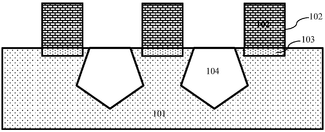
[0046] Before describing the embodiments of the present invention in detail, first introduce the manufacturing method of the existing NMOS tube, such as Figure 1A to Figure 1B What is shown is a device structure diagram in each step of the existing NMOS tube manufacturing method; the existing NMOS tube manufacturing method includes the following steps:

[0047] Step one, such as Figure 1A As shown, a silicon substrate with a P-well 101 formed on the surface is provided, a dummy gate structure is formed on the surface of the P-well 101, and the surface of the P-well 101 in the area covered by the dummy gate structure is used to form a channel 103.

[0048] The dummy gate structure includes a first gate dielectric layer formed on the surface of the P well 101 and a polysilicon dummy gate 102.

[0049] Silicon nitride sidewall spacers are formed on both sides of the dummy gate structure.

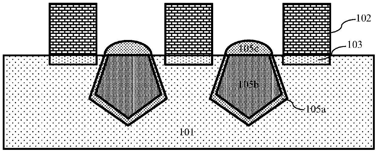
[0050] Step two, such as Figure 1A As shown, ...


PUM


Abstract

The invention discloses an NMOS tube which comprises a P well formed on a surface of a silicon substrate, a gate structure formed on a surface of the P well, grooves formed on two sides of the gate structure, and embedded epitaxial layers in the grooves. The embedded epitaxial layers comprise silicon seed layers, silicon phosphorous main body layers, silicon phosphorous buffer layers between the silicon phosphorous main body layers and the silicon seed layers, and silicon cap layers protruding to the tops of the grooves. The silicon phosphorous main body layers have phosphorus heavily-doped structures, the silicon phosphorous buffer layers have phosphorus lightly-doped structures and are used for reducing the number of phosphorus of the embedded epitaxial layers expanded to a peripheral side P well so as to reduce and prevent the influence of the expanded phosphorus on channels. The invention also discloses a manufacturing method of the NMOS tube. The short channel effect of a device can be improved, and therefore, the stability of the device is improved.

Description

Technical field [0001] The invention relates to the field of semiconductor integrated circuit manufacturing, in particular to an NMOS tube; the invention also relates to a method for manufacturing an NMOS tube. Background technique [0002] HKMG has a high dielectric constant (HK) gate dielectric layer and a metal gate (MG), so it is usually abbreviated as HKMG in the art. In MOS transistors using HKMG, the source and drain regions of NMOS often use embedded epitaxial layers. The material of the embedded epitaxial layer of NMOS is usually SiP. The embedded epitaxial layer changes the stress of the channel region of the NMOS and forms beneficial Improve the tensile stress of the electron mobility in the NMOS channel region, thereby improving the electron mobility in the NMOS channel region and reducing the channel resistance. [0003] With the development of technology, the critical dimension (CD) of the device is getting smaller and smaller. For example, the technology node of the...

Claims


Application Information

Patent Timeline
Patent Type & Authority Applications(China)
IPC IPC(8): H01L29/78H01L29/06H01L27/092H01L21/336
CPCH01L27/092H01L29/0642H01L29/0684H01L29/66545H01L29/66553H01L29/78
Inventor 陈品翰
Owner SHANGHAI HUALI INTEGRATED CIRCUTE MFG CO LTD
Why Eureka
Try Eureka