Supercharge Your Innovation With Domain-Expert AI Agents!

A high-efficiency conductive silver glue bonding wire sealing process for semiconductors

A technology of conductive silver glue and glue sealing process, which is applied in the manufacture of semiconductor/solid-state devices, semiconductor devices, circuits, etc., can solve the problems of time-consuming, reduce the qualified rate of finished products, and occupy manpower and man-hours, so as to speed up curing time and improve processing Efficiency and the effect of reducing labor occupation

Active Publication Date: 2020-10-23
惠州市鑫永诚光电科技有限公司
View PDF3 Cites 0 Cited by
  • Summary
  • Abstract
  • Description
  • Claims
  • Application Information

AI Technical Summary

Problems solved by technology

[0003] Most of the semiconductor die bonding and wire bonding methods currently used by packaging factories are the traditional silver glue baking method, that is, the staff removes the die bonded semiconductor from the die bonder and places it in the semiconductor storage box according to the specifications. , moved to the heating oven for heating, generally need to be baked for 2-3 hours, the specific baking time is adjusted according to the type of semiconductor and the selection of the adhesive colloid selected, after the baking is completed, it is used by the staff The special clamping tool transfers the semiconductor storage box. After the temperature of the original high-temperature semiconductor storage box drops to normal temperature, it is transferred to the wire bonding machine for wire bonding. The curing time of the silver glue used in the traditional semiconductor packaging process needs at least two hours. If the silver glue is not fully cured, it may lead to quality problems in the finished semiconductor. Therefore, professionals are required to check the curing of the silver glue. At the same time, special personnel are required to bake, bake and transfer the semiconductor to the bonding wire during semiconductor processing. The machine place takes up a lot of manpower and man-hours, which affects the processing efficiency of semiconductors, and due to the high error rate in the operation process of personnel, it is easy to cause some defective products in the finished product, reducing the pass rate of the finished product. Baking and transshipment are time-consuming, prolonging the production cycle of the product

Method used


Image

  • A high-efficiency conductive silver glue bonding wire sealing process for semiconductors

Examples


Embodiment 1

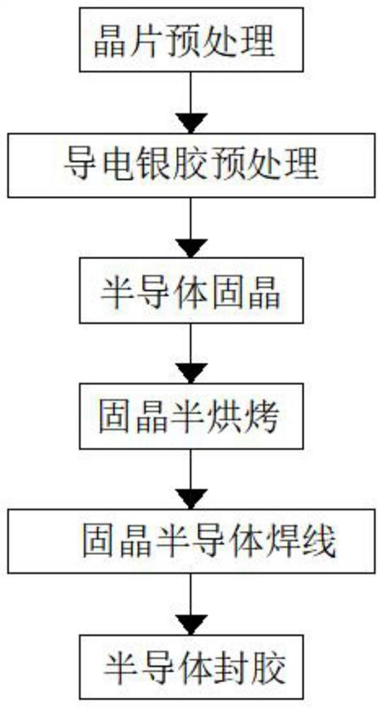
[0041] see figure 1 , a semiconductor high-efficiency conductive silver glue die-bonding wire sealing process, comprising the following steps:

[0042] Step 1: Chip pretreatment. After confirming the raw material specifications and batches after the warehouse feeds, the original chip is torn off the film. After the film is peeled off, the original chip is expanded. After the expansion is completed, the chip to be processed is obtained. , Step 1 During the chip pretreatment process, open the upper cover of the crystal expander, and place the inner ring of the crystal expander on the base flatly, with the smooth side facing up. The technicians tear off the centrifuge paper of the chip, with the centrifuge paper facing up and the blue film facing down. , to facilitate the complete expansion and deployment of the chip. In the pretreatment process of step 2 conductive silver glue, first thaw the bottle and syringe. The thawing time is 30 minutes. After thawing is completed, move th...


PUM


Abstract

The invention discloses a high-efficiency conductive silver glue die-bonding wire sealing process for a semiconductor, and belongs to the technical field of die-bonding wire welding. The process comprises the following steps: chip preprocessing, conducive silver glue preprocessing, semiconductor die bonding, die bonding semi-baking, die bonding semiconductor wire welding, and semiconductor glue sealing. The reconstruction of a discharge device of a conventional die bonding machine can be achieved, and a material box loaded with a die bonding semiconductor semi-finished product is pushed through a material pushing cylinder, and then enters to a conveying chain of a die bonding region, thereby reducing the manpower for the laying-off after die bonding, the transferring before baking, the transferring after baking, the transferring after wire welding and glue sealing to reduce the manpower cost, shortening the baking time of the silver glue, improving the processing efficiency of the semiconductor, reducing the energy consumption, reducing the error rate of manual operation, and improving the qualified rate of finished products.

Description

technical field [0001] The invention relates to the technical field of crystal bonding wires, and more specifically relates to a high-efficiency conductive silver glue bonding wire sealing process for semiconductors. Background technique [0002] Solid crystal is also known as DieBond or chip loading. Die bonding is the process of bonding the chip to the designated area of ​​the bracket through colloid (for LEDs, generally conductive glue or insulating glue) to form a thermal path or electrical path, and provide conditions for subsequent wiring connections. [0003] Most of the semiconductor die bonding and wire bonding methods currently used by packaging factories are the traditional silver glue baking method, that is, the staff removes the die bonded semiconductor from the die bonder and places it in the semiconductor storage box according to the specifications. , moved to the heating oven for heating, generally need to be baked for 2-3 hours, the specific baking time is ...

Claims


Application Information

Patent Timeline
Patent Type & Authority Patents(China)
IPC IPC(8): H01L33/52H01L33/62H01L21/02H01L21/67H01L21/677
CPCH01L21/02068H01L21/02096H01L21/67253H01L21/67736H01L33/52H01L33/62H01L2933/005H01L2933/0066
Inventor 吴伟谭起富彭超
Owner 惠州市鑫永诚光电科技有限公司
Features
  • R&D
  • Intellectual Property
  • Life Sciences
  • Materials
  • Tech Scout
  • Unparalleled Data Quality
  • Higher Quality Content
  • 60% Fewer Hallucinations
Learn More