Fabry-Perot antenna with high gain and low radar cross section
A radar cross-section, high-gain technology, applied in the field of high-gain, communication antennas and missile antennas, and low radar cross-section Fabry-Perot antennas, can solve the problems of poor gain enhancement effect and poor radar cross-section reduction effect, to overcome The surrounding structure is complex, reducing the metal strip structure, and overcoming the effect of poor gain enhancement effect
- Summary
- Abstract
- Description
- Claims
- Application Information
AI Technical Summary
Problems solved by technology
Method used
Image
Examples
Embodiment 1
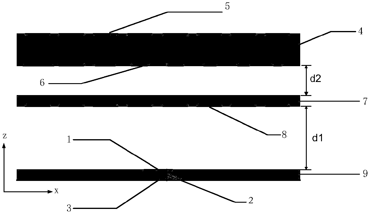
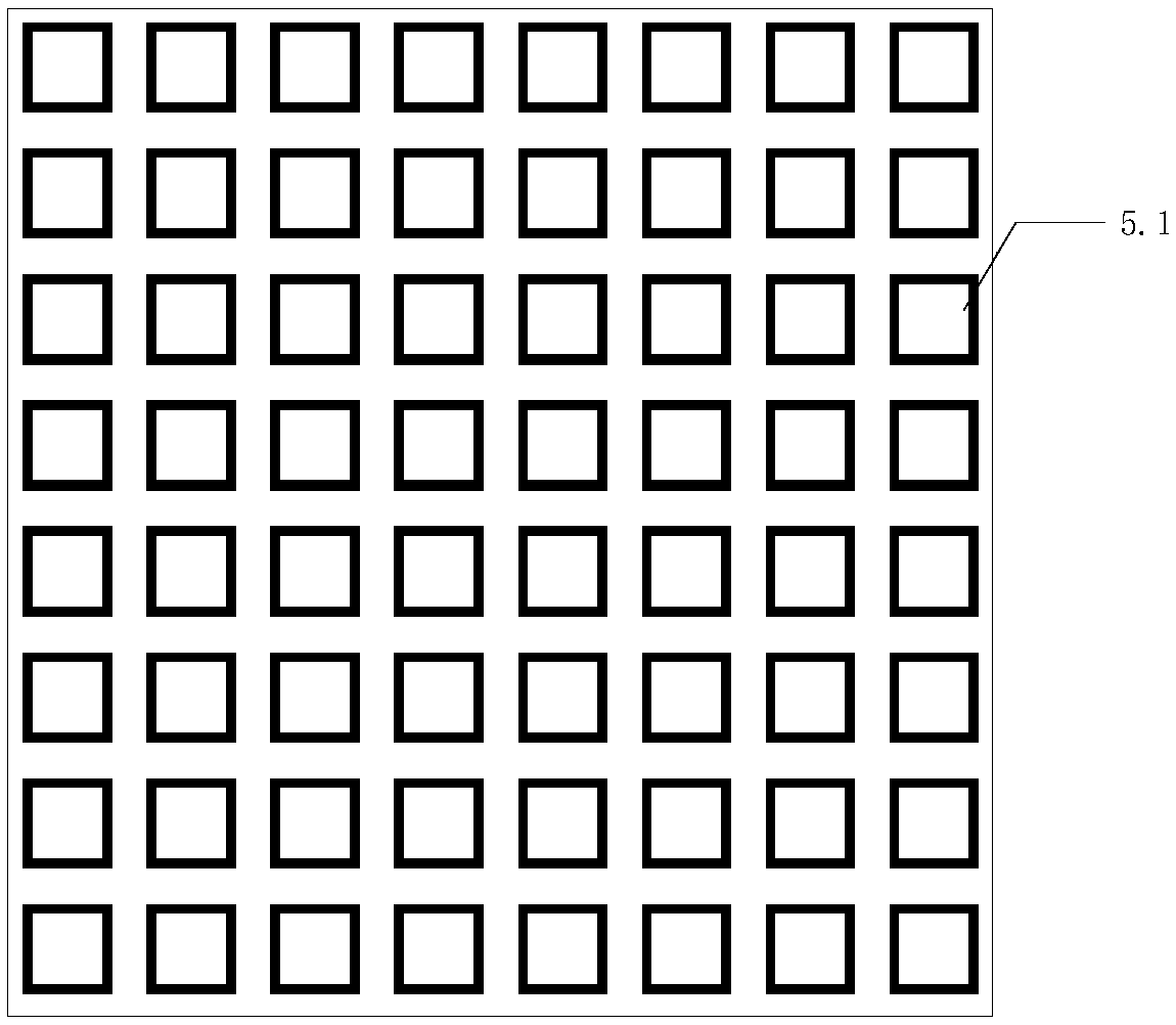
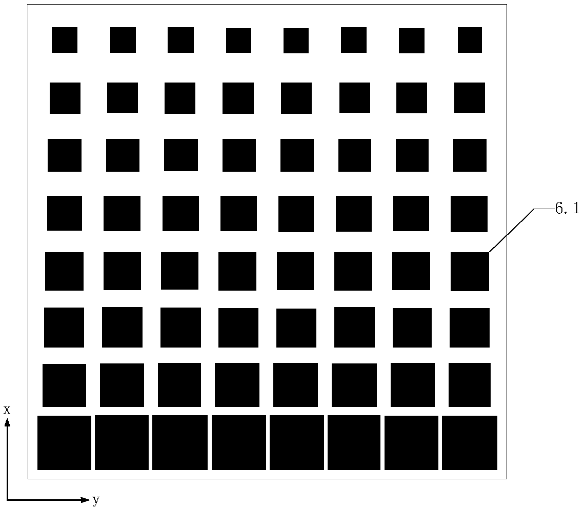
[0031] refer to figure 1 , figure 2 , image 3 and Figure 4 ,
[0032] A Fabry-Perot antenna with high gain and low radar cross section, comprising an antenna radiator 1, a feed structure 2, a metal floor 3, and a first wave-absorbing coating printed on the upper and lower surfaces of a first dielectric substrate 4 5. The second reflective coating 6 and the third reflective coating 8 printed on the lower surface of the second dielectric substrate 7; the antenna radiator 1 is printed on the upper surface of the third dielectric substrate 9, and the feeding structure 2 Penetrating through the third dielectric substrate 9 and connected to the antenna radiator 1 and the metal floor 3, the first wave-absorbing cladding 5 is distributed in a checkerboard pattern, and is composed of N×N square absorbers with the same structure periodically arranged Composed of unit 5.1, wherein, N≥2, N is a positive integer, each square absorbing unit 5.1 is a metal ring structure, and the four...
Embodiment 2
[0046] This embodiment has the same structure as Embodiment 1, only the following parameters are adjusted:
[0047] refer to figure 1
[0048] The thickness of the air layer between the second dielectric substrate and the third dielectric substrate is d1, d1=10mm, the thickness of the air layer between the first dielectric substrate and the second dielectric substrate is d2, d2=0.2mm
[0049] refer to Figure 5
[0050] Square metal ring patch unit 8.1, when the outer length is Wout=9mm, the width of the metal ring is Ws, Ws=2mm. The side length of the square metal patch unit is Wm=2mm, the side length of the square metal ring on the square absorbing unit 5.1 is a=3mm, and the width of the metal ring is W1=0.1mm.
Embodiment 3
[0052] This embodiment has the same structure as Embodiment 1, only the following parameters are adjusted:
[0053] refer to figure 1
[0054] The thickness of the air layer between the second dielectric substrate and the third dielectric substrate is d1, d1=26mm, the thickness of the air layer between the first dielectric substrate and the second dielectric substrate is d2, d2=1.8mm
[0055] refer to Figure 5
[0056] Square metal ring patch unit 8.1, when the outer side length is Wout=17mm, the width of the metal ring is Ws, Ws=6mm. The side length Wm=17mm of the square metal patch unit, the side length a=9mm of the square metal ring on the square absorbing unit 5.1, the width of the metal ring is W1, W1=1.1mm.
[0057] Below in conjunction with accompanying drawing and the present invention will be further described
[0058] Simulation content and conditions
[0059] refer to Figure 7 , the present invention simulates the antenna in Embodiment 1 through the electro...
PUM
 Abstract
Description
Claims
Application Information


