Chip contact assembly and consumable container

A technology for contacting components and consumable containers, applied in instruments, electrical recordings, optics, etc., can solve problems such as poor contact between chips and electrical connections, and achieve good electrical connections

Pending Publication Date: 2019-04-05
PRINT RITE UNICORN IMAGE PROD CO LTD
View PDF0 Cites 2 Cited by
  • Summary
  • Abstract
  • Description
  • Claims
  • Application Information

AI Technical Summary

Problems solved by technology

[0002] A detachable consumable container is usually arranged in an existing printer or copier, such as a developer cartridge installed in a laser printer. Usually, the developer cartridge has a housing on which a chip is installed,

Method used


Image

  • Chip contact assembly and consumable container
  • Chip contact assembly and consumable container
  • Chip contact assembly and consumable container

Examples


Embodiment 1

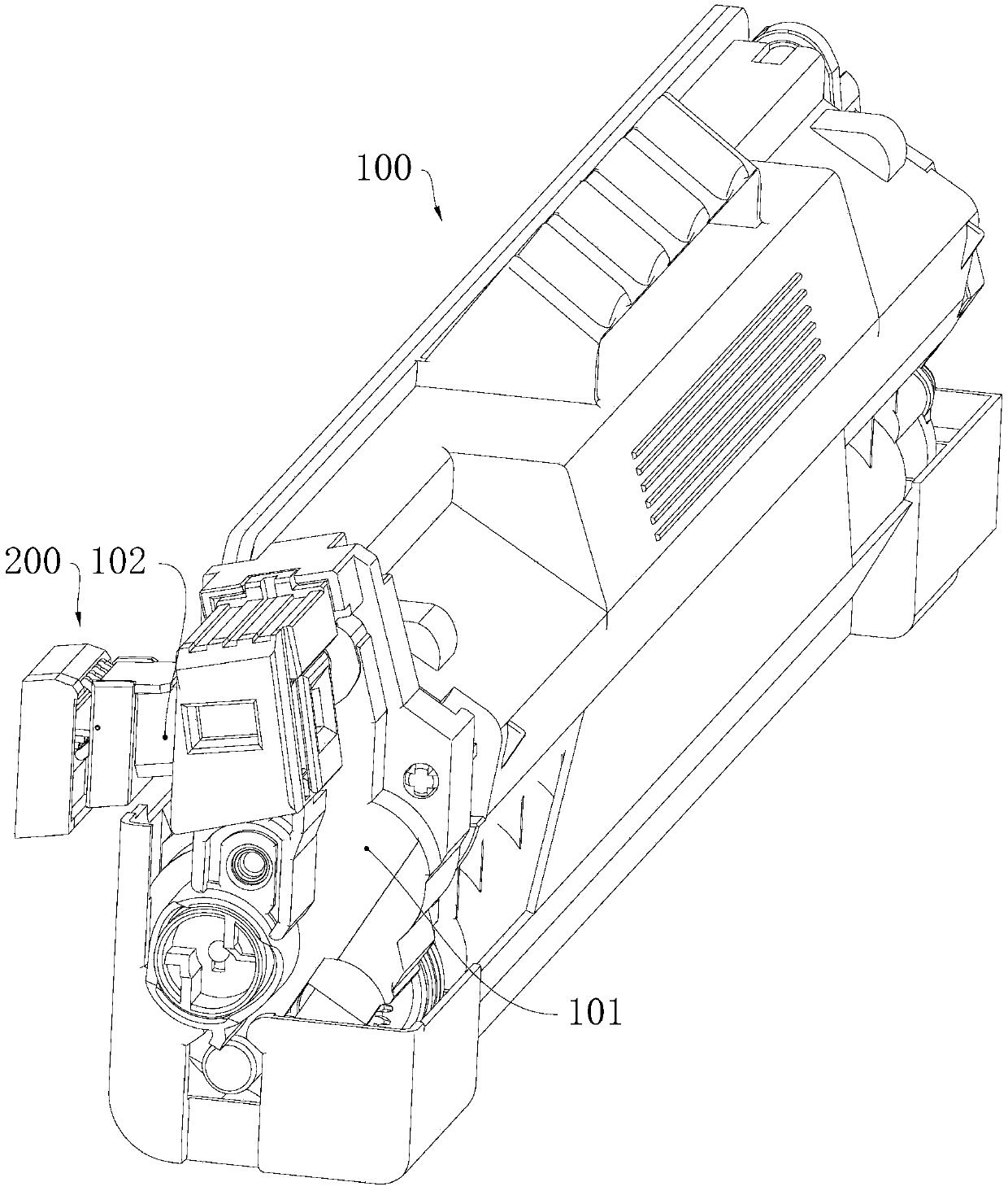
[0026] The consumable container, such as the ink cartridge or the developer cartridge 100, can be used in a printer or a copier. In this embodiment, the application of the chip contact assembly and the consumable container to a laser printer is taken as an example.

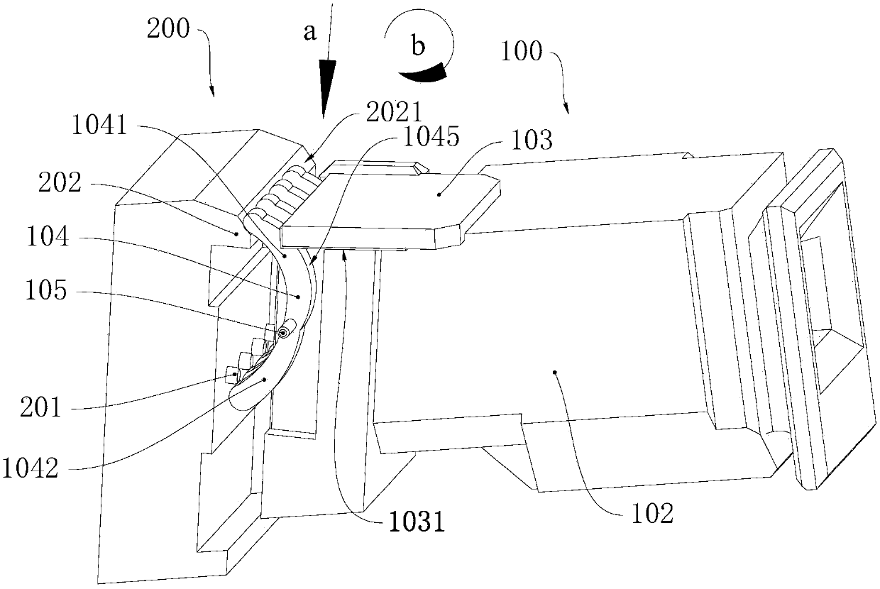
[0027] The laser printer has a body 200 and a developer cartridge 100, the developer cartridge 100 is mounted on the body 200, and the direction in which the developer cartridge 100 is inserted into the body 200 is set as a first direction a.

[0028] Please refer to Figure 1 to Figure 2 , the body 200 is provided with an abutment portion 202 and an electrical connection portion 201, along the first direction a, the abutment portion 202 is located behind the electrical connection portion 201, and the abutment portion 202 is provided with a guide surface 2021, along the first direction a , The guide surface 2021 is inclined toward the developing cartridge 100 side.

[0029] The developing cartridge 100 includes a...

Embodiment 2

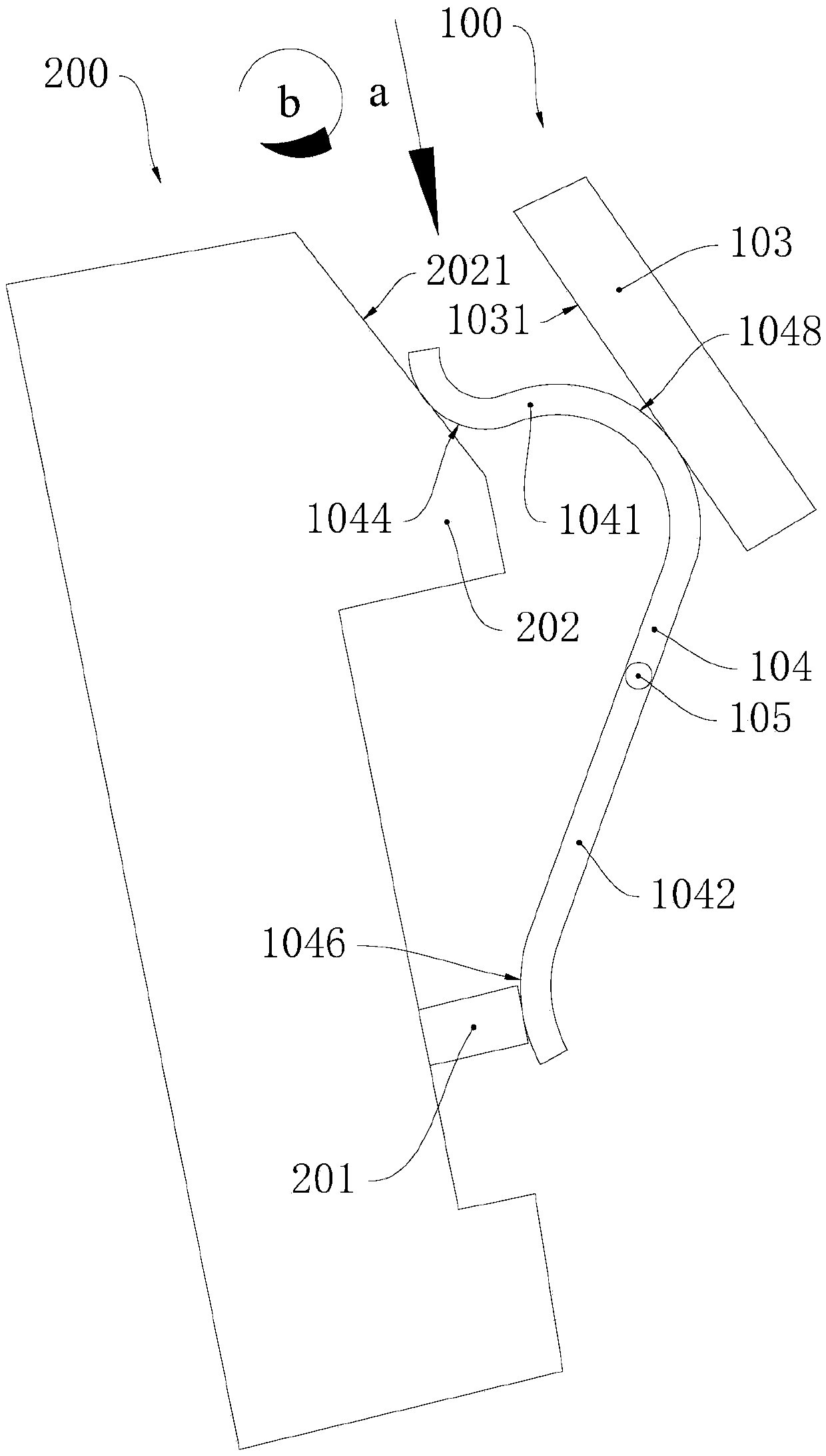
[0041] Please refer to image 3 , the connecting contact pin 104 is made into three curved waves, the wavy connecting contact pin 104 has a convex arc surface 1044, a convex arc surface 1048 and a convex arc surface 1046, and the guiding surface of the convex arc surface 1044 and the contact part 202 2021 abuts, the convex arc surface 1048 abuts against the electrical contact surface 1031 of the chip 103 , and the convex arc surface 1046 abuts against the electrical connection portion 201 .

[0042] Other parts of the second embodiment of the chip contact assembly and the consumable container are the same as the first embodiment of the chip contact assembly and the consumable container.

Embodiment 3

[0044] Please refer to Figure 4 , the connection contact pin 104 may also have a third leg 1043, the first leg 1041 of the connection contact pin 104 abuts against the electrical contact surface 1031 of the chip 103, the second leg 1042 of the connection contact pin 104 abuts against the electrical connection portion 201, The third leg 1043 connecting the contact pin 104 abuts against the abutting portion 202 on the printer body 200 .

[0045] In the case of setting the third leg 1043, the first leg 1041 and the chip 103 can always be kept inside the chip seat 102, and the third leg 1043 protrudes out of the chip seat 102, and is inserted into the developing cartridge 100 along the first direction a into the machine body In the process of 200, the third leg 1043 abuts against the abutment portion 202, under the abutment of the abutment portion 202, the connecting contact pin 104 rotates until the first leg 1041 abuts against the electrical contact surface 1031 of the chip 103...


PUM


Abstract

The invention relates to the technical field of electronic shooting. A chip contact assembly provided by the invention comprises a first matrix, a chip and a connection contact pin and also comprisesa connection touch pin, wherein the chip is fixedly arranged on the first matrix and is provided with an electrical contact surface, the connection contact pin is provided with a first leg and a second leg, the connection contact pin is hinged with the first matrix, and the electrical contact surface is arranged on a rotation path of the first leg. A consumable container provided by the inventioncomprises the chip contact assembly. The connection contact pin is hinged with the first matrix, the electrical contact surface of the chip is arranged on the rotation path of the first leg, thus, theexternal matrix props against the connection contact pin to rotate when the chip is connected with an external electrical connection part, the first leg props against the electrical contact surface of the chip, the second leg props against the external electrical connection part, the electrical contact surface of the external electrical connection part and the chip can be electrically connected by the connection contact pin, and favorable electrical connection between the chip and the external electrical connection part is facilitated.

Description

technical field [0001] The invention relates to the technical field of electrophotography, in particular to a chip contact assembly and a container for consumables. Background technique [0002] A detachable consumable container is usually arranged in an existing printer or copier, such as a developer cartridge installed in a laser printer. Usually, the developer cartridge has a housing on which a chip is installed, and the electrical connection between the chip and the printer However, after the developing cartridge is installed in the printer, poor contact between the chip and the electrical connection is prone to occur. Contents of the invention [0003] The main object of the present invention is to provide a chip contact assembly which facilitates good contact between the chip and the electrical connection. [0004] In order to achieve the above-mentioned main purpose, the chip contact assembly provided by the present invention includes a first substrate, a chip and ...

Claims


Application Information

Patent Timeline
IPC IPC(8): G03G15/08G03G15/00
CPCG03G15/0863G03G15/80
Inventor 杨晓锋何永刚
Owner PRINT RITE UNICORN IMAGE PROD CO LTD
Why Eureka
Try Eureka