
Shift register units, drive method thereof, gate driver circuits and display device
A shift register and circuit technology, applied in the fields of shift register units and driving methods, gate drive circuits, and display devices, can solve problems such as increased power consumption of products and extra power consumption generated by shift register units.
- Summary
- Abstract
- Description
- Claims
- Application Information
AI Technical Summary
Problems solved by technology
Method used
Image

Examples
Embodiment 1
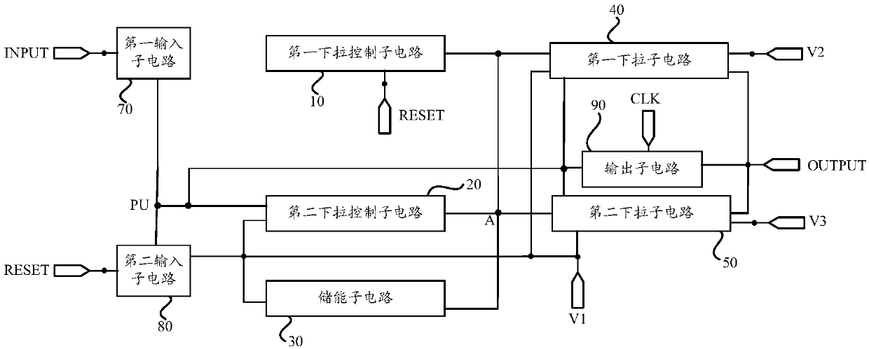
[0100] Such as Figure 6 and Figure 9 As shown, the first pull-down control sub-circuit 10 includes a first transistor M1; the gate of the first transistor M1 is connected to the reset signal terminal RESET, the first pole of the first transistor M1 is connected to the reset signal terminal RESET, and the first electrode of the first transistor M1 is connected to the reset signal terminal RESET. The two poles are connected between the energy storage sub-circuit 30 and the selection node A.
[0101] The second pull-down control sub-circuit 20 includes a second transistor M2; the gate of the second transistor M2 is connected to the pull-up node PU, the first pole of the second transistor M2 is connected to the energy storage sub-circuit 30 and the selection node A, and the gate of the second transistor M2 is connected to the pull-up node PU. The second pole is connected to the first voltage terminal V1.
[0102] The energy storage sub-circuit 30 includes a first capacitor C1,...
Embodiment 2
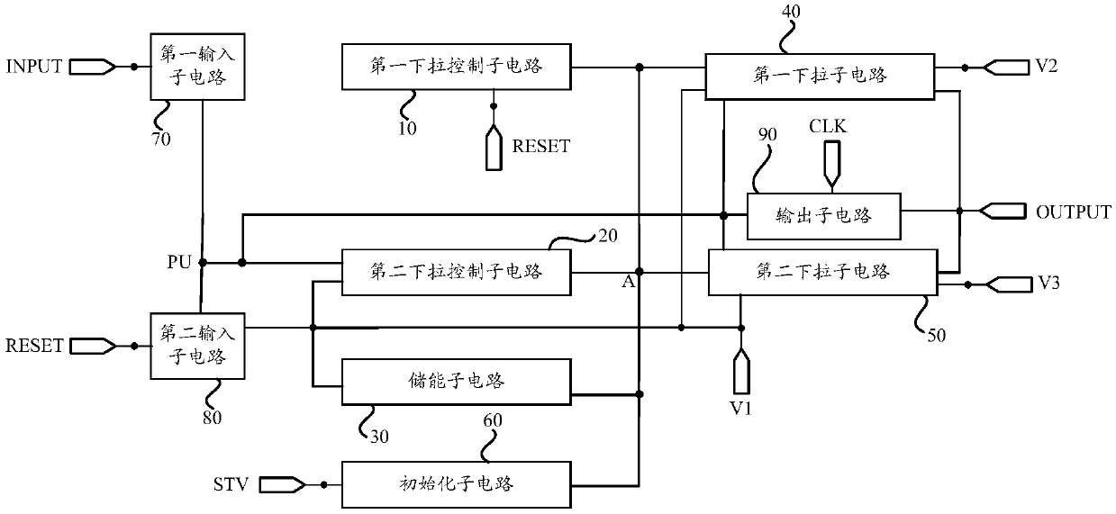
[0119] Such as Figure 7 and Figure 10 As shown, the first pull-down control sub-circuit 10 includes a first transistor M1; the gate of the first transistor M1 is connected to the reset signal terminal RESET, the first pole of the first transistor M1 is connected to the reset signal terminal RESET, and the first electrode of the first transistor M1 is connected to the reset signal terminal RESET. The two poles are connected between the energy storage sub-circuit 30 and the selection node A.
[0120] The second pull-down control sub-circuit 20 includes a second transistor M2; the gate of the second transistor M2 is connected to the pull-up node PU, the first pole of the second transistor M2 is connected to the energy storage sub-circuit 30 and the selection node A, and the gate of the second transistor M2 is connected to the pull-up node PU. The second pole is connected to the first voltage terminal V1.
[0121] The energy storage sub-circuit 30 includes a first capacitor C1...
PUM
 Abstract
Description
Claims
Application Information