Anisotropic conductive adhesive

An anisotropic, conductive adhesive technology, applied in the direction of conductive adhesives, adhesives, film/sheet adhesives, etc., can solve the problems of easy generation of binding bubbles, easy generation of attachment bubbles, etc., to achieve improved adhesion The effect of attaching quality or binding quality and improving reliability

Inactive Publication Date: 2019-04-16
WUHAN CHINA STAR OPTOELECTRONICS SEMICON DISPLAY TECH CO LTD
View PDF8 Cites 0 Cited by
  • Summary
  • Abstract
  • Description
  • Claims
  • Application Information

AI Technical Summary

Problems solved by technology

[0005] The purpose of the present invention is to provide an anisotropic conductive adhesive, which can solve the problems that existing anisotropic conductive adhesives are easy to generate sticking bubbles when attaching, and easy to generate binding bubbles after binding under pressure.

Method used


Image

  • Anisotropic conductive adhesive
  • Anisotropic conductive adhesive
  • Anisotropic conductive adhesive

Examples


Embodiment 1

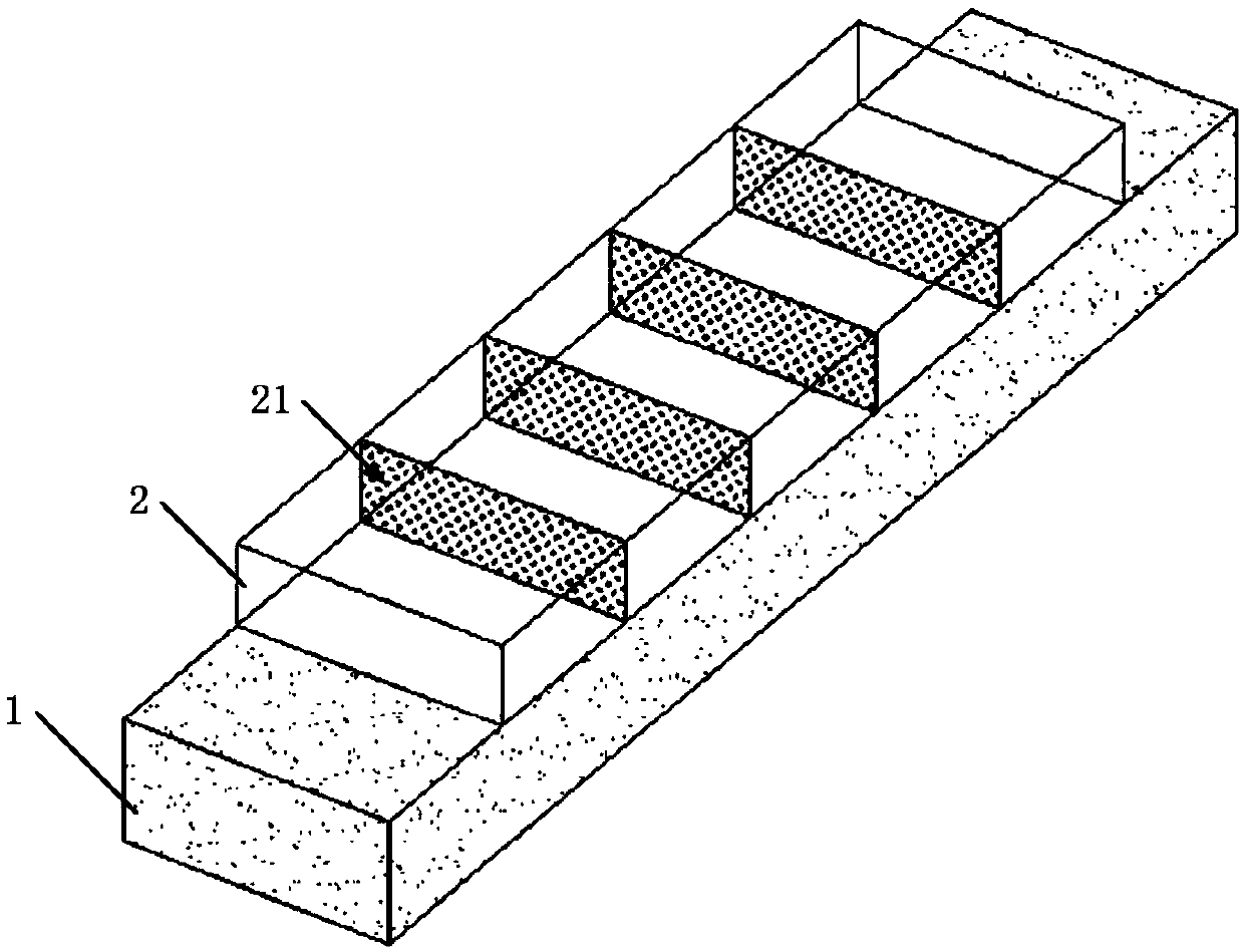
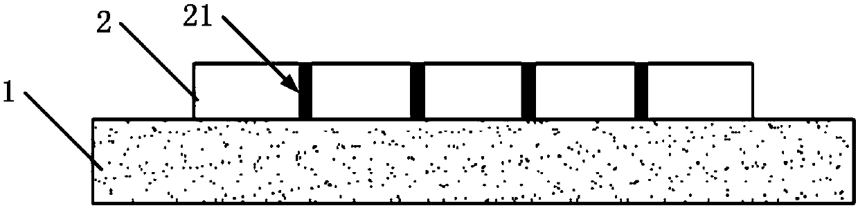
[0033] Such as figure 1 As shown, the perspective view of the anisotropic conductive adhesive in Example 1 includes a substrate 1 and an adhesive layer 2 disposed on the substrate 1 . The adhesive layer 2 is provided with a groove 21 , and the groove 21 penetrates downward through the adhesive layer 2 to the upper surface of the substrate 1 . Specifically, the through hole 21 can be provided by a die-cutting method.

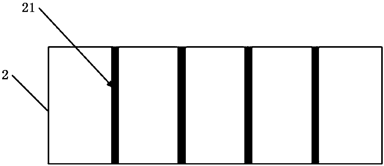
[0034] Such as figure 2 As shown in the top view of the anisotropic conductive adhesive in Example 1, the grooves 21 are parallel to each other, and the distances between the grooves 21 are the same, forming a grid array. Wherein the groove 21 is parallel to the short side direction of the adhesive layer 2 . The anisotropic conductive adhesive thus formed can well discharge the attachment air bubbles that are easily generated during attachment and the binding air bubbles that are easily generated after the pressure binding through the groove 21, thereby improv...

Embodiment 2

[0039] Such as Figure 4 As shown, the perspective view of the anisotropic conductive adhesive in Example 2 includes a substrate 1 and an adhesive layer 2 disposed on the substrate 1 . The adhesive layer 2 is provided with a groove 21 , and the groove 21 penetrates downward through the adhesive layer 2 to the upper surface of the substrate 1 . Specifically, the through hole 21 can be provided by a die-cutting method.

[0040] Such as Figure 5 As shown in the top view of the anisotropic conductive adhesive in Example 2, the grooves 21 are parallel to each other, and the distances between the grooves 21 are the same, forming a grid array. Wherein the groove 21 is arranged obliquely with respect to the short side direction of the adhesive layer 2 , preferably, the angle between the groove 21 and the short side direction of the adhesive layer 2 can be set as 45 degrees. The anisotropic conductive adhesive thus formed can well discharge the attachment air bubbles that are easily...


PUM


Abstract

The invention relates to an anisotropic conductive adhesive. The conductive adhesive comprises a substrate and an adhesive layer arranged on the substrate. The surface of the adhesive layer is sunkendownwards to penetrate through the adhesive layer till a groove is formed in the upper surface of the substrate, wherein one end of the groove extends out of the edge of the adhesive layer. Accordingto the anisotropic conductive adhesive, due to the groove and a channel formed by the port, extending out of the edge of the adhesive layer, of the groove and the external world, attaching bubbles aregenerated during attaching, and binding bubbles generated by binding can be exhausted out of the adhesive layer through the channel, so that the attaching quality or the binding quality is improved,and then, the product reliability is improved.

Description

technical field [0001] The invention relates to an anisotropic conductive adhesive, which is used for the connection between semiconductor electronic components, for example, the connection between related module components in a display panel. Background technique [0002] With the development of the times, in the modern communication industry, the market demand for mobile phones, TVs, tablets, notebooks, digital cameras and other products is increasing, and various display devices are also developing towards high resolution. In the existing display module manufacturing, there is a process of binding components to the module; in the component binding process, an anisotropic conductive film (ACF, Anisotropic Conductive Film) is used to connect the components . [0003] The anisotropic conductive adhesive is characterized in that the Z-axis electrical conduction direction is significantly different from the resistance characteristics of the XY insulating plane. When the diff...

Claims


Application Information

Patent Timeline
IPC IPC(8): C09J7/20C09J9/02
CPCC09J7/20C09J9/02C09J2301/122C09J2301/204C09J2301/312C09J2301/314
Inventor 祝翠林
Owner WUHAN CHINA STAR OPTOELECTRONICS SEMICON DISPLAY TECH CO LTD
Why Eureka
Try Eureka