An optical bistable device for all-optical switches and optical memories
What is AI technical title?
AI technical title is built by PatSnap AI team. It summarizes the technical point description of the patent document.
A technology of bistable devices and all-optical switches, applied in the field of all-optical communication systems, to achieve the effect of enhancing the third-order nonlinear effect and reducing the threshold
Active Publication Date: 2022-03-11
HUBEI UNIV OF SCI & TECH
View PDF5 Cites 2 Cited by
Summary
Abstract
Description
Claims
Application Information
AI Technical Summary
This helps you quickly interpret patents by identifying the three key elements:
Problems solved by technology
Method used
Benefits of technology
Problems solved by technology
And SPPs can only be excited in metamaterials and Kretschmann structures
Method used
Image
Click on the blue label to locate the original text in one second.
Reading with bidirectional positioning of images and text.
Examples
Embodiment Construction
[0038] The following are specific embodiments of the present invention and in conjunction with the accompanying drawings, the technical solutions of the present invention are further described, but the present invention is not limited to these embodiments.
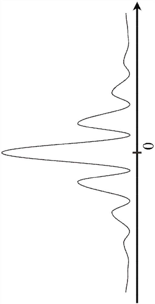
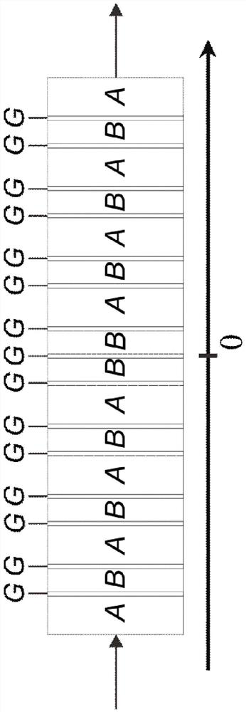
[0039] Such as figure 1As shown, the optical bistable device is a multilayer structure composed of eight dielectric layers A, eight dielectric layers B and fifteen graphene layers G, and the optical bistable device is from the upper surface to the lower surface Dielectric layer one A, graphene layer G, dielectric layer two B, graphene layer G, dielectric layer one A, graphene layer G, dielectric layer two B, graphene layer G, dielectric layer one A, graphene layer G, dielectric layer two B, graphene layer G, dielectric layer one A, graphene layer G, dielectric layer two B, graphene layer G, dielectric layer two B, graphene layer G, dielectric layer one A, graphene layer G, dielectric layer two B, graphene layer G, dielect...
PUM
Property
Measurement
Unit
thickness
aaaaa
aaaaa
thickness
aaaaa
aaaaa
refractive index
aaaaa
aaaaa
Abstract
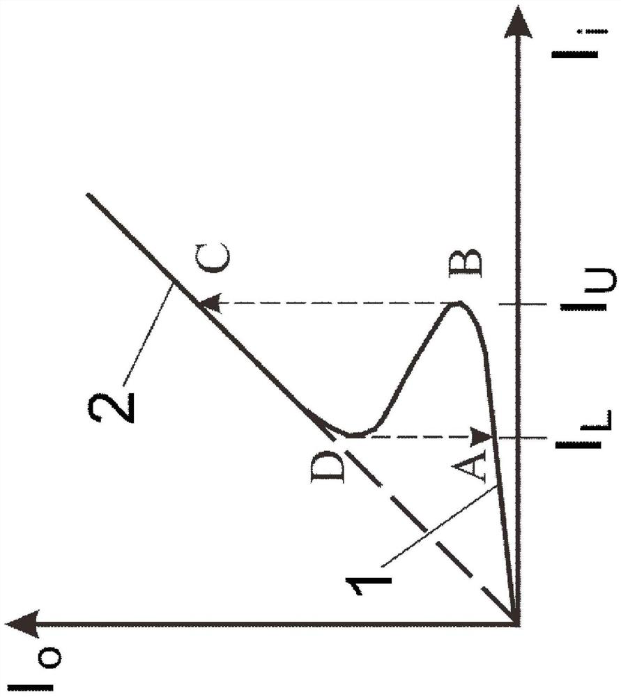
The invention provides an optical bistable device applied to an all-optical switch and an optical memory, and belongs to the technical field of all-optical communication systems. The optical bistable device is a multilayer structure composed of eight dielectric layers 1, eight dielectric layers 2 and fifteen graphene layers. From the upper surface to the lower surface, there are dielectric layer 1, graphene layer, dielectric layer 2, Graphene layer, Dielectric layer 1, Graphene layer, Dielectric layer 2, Dielectric layer 1, Graphene layer, Dielectric layer 2, Dielectric layer 1, Graphene layer, Dielectric layer 2, Graphene layer, Dielectric layer 2, Graphene layer, dielectric layer one, graphene layer, dielectric layer two, graphene layer, dielectric layer one, graphene layer, dielectric layer two, graphene layer, dielectric layer one, graphene layer, dielectric layer two, graphene layer, Dielectric layer one. The invention has the advantages of being able to reduce the threshold of the optical bistable state and the like.
Description
technical field [0001] The invention belongs to the technical field of all-optical communication systems, and relates to an optical bistable device applied to all-optical switches and optical memories. Background technique [0002] With the development of all-optical network and information detection technology, there is an urgent need to develop all-optical switches and optical memories. The material-based optical bistability effect can realize all-optical switches and optical memories. [0003] In the past, surface plasmon polaritons (SPPs) or Fabry-Perot cavity structures were generally used to enhance the localization of the electric field, and then materials with large nonlinear coefficients were used to achieve low-threshold optical dual steady state. [0004] SPPs require TM waves to be generated in metals or graphene, and SPPs only go along the surface of the material. Moreover, SPPs can only be excited in metamaterials and Kretschmann structures. [0005] As an ...
Claims
Application Information
Patent Timeline
Application Date:The date an application was filed.
Publication Date:The date a patent or application was officially published.
First Publication Date:The earliest publication date of a patent with the same application number.
Issue Date:Publication date of the patent grant document.
PCT Entry Date:The Entry date of PCT National Phase.
Estimated Expiry Date:The statutory expiry date of a patent right according to the Patent Law, and it is the longest term of protection that the patent right can achieve without the termination of the patent right due to other reasons(Term extension factor has been taken into account ).
Invalid Date:Actual expiry date is based on effective date or publication date of legal transaction data of invalid patent.

