Array substrate and preparation method thereof, and display panel

An array substrate and array arrangement technology, applied in the direction of semiconductor devices, electrical components, circuits, etc., can solve problems such as adverse effects on users' visual experience, poor display effect of display panels, and poor display effect of sub-pixels, etc., to improve the display. effect, ensure high PPI, avoid the effect of crosstalk

Active Publication Date: 2021-04-30
WUHAN TIANMA MICRO ELECTRONICS CO LTD
View PDF3 Cites 0 Cited by
  • Summary
  • Abstract
  • Description
  • Claims
  • Application Information

AI Technical Summary

Problems solved by technology

[0004] However, when multiple sub-pixels in the same display pixel receive different voltages, the sub-pixels will be affected by the voltage of adjacent sub-pixels, resulting in poor display effect of the affected sub-pixels, thus making the display panel The display effect of the display is not good, which has a bad influence on the user's visual experience

Method used


Image

  • Array substrate and preparation method thereof, and display panel
  • Array substrate and preparation method thereof, and display panel
  • Array substrate and preparation method thereof, and display panel

Examples


Embodiment Construction

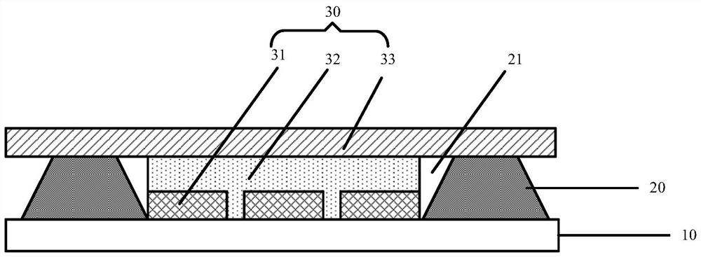
[0044] In the prior art, a display pixel is set as a reference for the cross-sectional structure of an array substrate that emits multiple sub-pixels of the same color light figure 1 ,exist figure 1 In the shown array substrate, a substrate 10 and a pixel definition layer 20 located on the substrate are shown, the pixel definition layer is provided with a plurality of pixel grooves 21 arranged in an array, and each pixel groove 21 is A plurality of anodes 31 , a light-emitting layer 32 covering the anodes 31 and a whole cathode 33 covering the light-emitting layer 32 are provided; the plurality of anodes 31 share the same light-emitting layer 32 and cathode 33 to form a plurality of sub-pixels 30 . Since the light-emitting layer 32 is a conductive structure, when the anode 31 of a sub-pixel in the same pixel groove 21 receives a voltage, it will affect the adjacent sub-pixels through the shared light-emitting layer 32, so that these sub-pixels It is difficult for pixels to ac...


PUM


Abstract

The present application discloses an array substrate, its preparation method, and a display panel, wherein, the array substrate is provided with at least one isolation mesa in the pixel groove in the pixel definition layer, so that the second sub-pixel located on the isolation mesa The light-emitting layer of the first sub-pixel and the light-emitting layer of the first sub-pixel located on the exposed bottom surface of the pixel groove are on different planes, thereby achieving the purpose of isolating the light-emitting layer of the second sub-pixel from the light-emitting layer of the first sub-pixel and avoiding the second When the anode of the sub-pixel and the anode of the first sub-pixel receive different voltages, the light-emitting layer affects the adjacent sub-pixels, which improves the display effect of the sub-pixels; and the isolation mesa arranged in the pixel groove is The coverage of the light-emitting layer of the second sub-pixel will not form a non-light-emitting area in the pixel groove, and will not reduce the aperture ratio of the array substrate. On the basis of avoiding the influence of crosstalk between adjacent sub-pixels, the high density of the array substrate is guaranteed. PPI.

Description

technical field [0001] The present application relates to the field of display technology, and more specifically, to an array substrate, a manufacturing method thereof, and a display panel. Background technique [0002] With the continuous development of display technology, the application of display panels is becoming more and more extensive. Self-luminous display panels refer to the display pixels on the array substrate composed of active light-emitting units, which can emit light without backlight excitation. , so as to realize the display of the screen, so that the backlight module of the display device can be removed, which is beneficial to reduce the overall thickness of the display device. [0003] An organic light emitting (Organic Light Emitting Diode, OLED) display panel is a kind of self-luminous display panel, and the OLED display panel has the advantages of fast response speed, brilliant color, thinness and convenience. In order to increase the PPI (Pixels Per ...

Claims


Application Information

Patent Timeline
Patent Type & Authority Patents(China)
IPC IPC(8): H01L27/32
CPCH10K59/12H10K59/1201H10K59/353H10K59/122H10K59/124H10K50/813H10K71/00H01L27/1218H01L27/1262H01L27/1288
Inventor 霍思涛
Owner WUHAN TIANMA MICRO ELECTRONICS CO LTD
Why Eureka
Try Eureka