Ingaas detector chip and preparation method thereof

A detector chip and absorbing layer technology, which is applied in the field of InGaAs detector chip and its preparation, can solve the problems of reduced chip life, chip failure, and normal use of customers, so as to increase junction capacitance, improve antistatic ability, and ensure reliability effect

Active Publication Date: 2020-07-28
SUZHOU SUNA PHOTOELECTRIC
View PDF6 Cites 0 Cited by
  • Summary
  • Abstract
  • Description
  • Claims
  • Application Information

AI Technical Summary

Problems solved by technology

[0003] However, in the fields of lasers, detectors and other chips, electrostatic breakdown often leads to the failure of the chip during use, resulting in a reduction in the life of the chip, affecting the normal use of customers, and the antistatic ability and reliability of the chip cannot be guaranteed.

Method used


Image

  • Ingaas detector chip and preparation method thereof
  • Ingaas detector chip and preparation method thereof
  • Ingaas detector chip and preparation method thereof

Examples


preparation example Construction

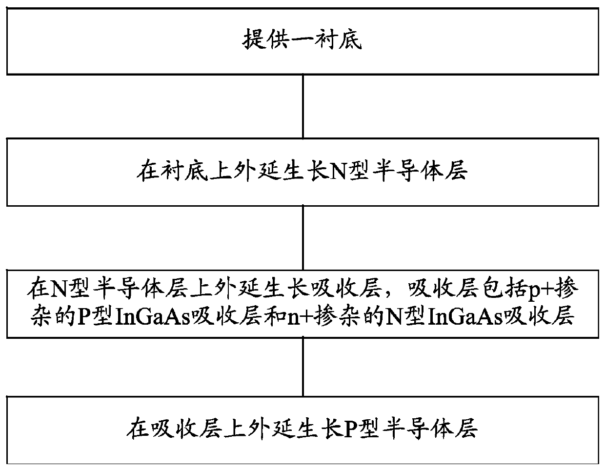
[0030] ginseng figure 2 As shown, the present invention also discloses a method for preparing an InGaAs detector chip, comprising:

[0031] providing a substrate;

[0032] epitaxially growing an N-type semiconductor layer on the substrate, the N-type semiconductor layer being an n+ doped InP layer;

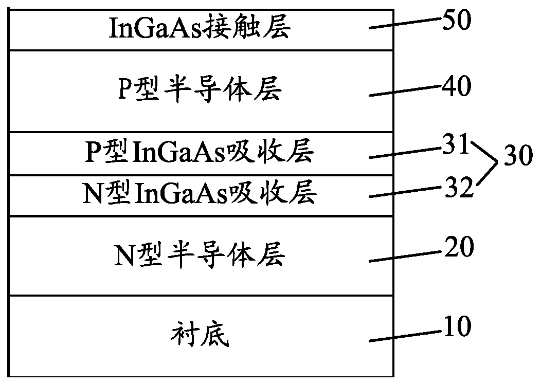
[0033] The absorber layer is epitaxially grown on the N-type semiconductor layer. The absorber layer includes a p+ doped P-type InGaAs absorber layer and an n+ doped N-type InGaAs absorber layer. The P-type InGaAs absorber layer is located above the N-type InGaAs absorber layer, and the P-type InGaAs The thickness of the absorbing layer is smaller than the thickness of the N-type InGaAs absorbing layer, and the doping concentration of the P-type InGaAs absorbing layer is greater than that of the N-type InGaAs absorbing layer;

[0034] A P-type semiconductor layer is epitaxially grown on the absorption layer, and the P-type semiconductor layer is a p+ doped InP layer.


PUM

PropertyMeasurementUnit
thicknessaaaaaaaaaa
thicknessaaaaaaaaaa
thicknessaaaaaaaaaa

Abstract

The invention discloses an InGaAs detector chip and a preparation method thereof. The InGaAs detector chip sequentially includes a substrate, an N-type semiconductor layer, an absorption layer, and a P-type semiconductor layer, and the N-type semiconductor layer is n+ doped The P-type semiconductor layer is a p+-doped InP layer, and the absorber layer includes a p+-doped P-type InGaAs absorber layer and an n+-doped N-type InGaAs absorber layer, and the P-type InGaAs absorber layer is in phase with the P-type semiconductor layer Adjacent, the N-type InGaAs absorbing layer is adjacent to the N-type semiconductor layer, the thickness of the P-type InGaAs absorbing layer is smaller than the thickness of the N-type InGaAs absorbing layer, and the doping concentration of the P-type InGaAs absorbing layer is greater than that of the N-type InGaAs absorbing layer. impurity concentration. The present invention optimizes the thickness and doping of the absorbing layer, adopts two layers of InGaAs absorbing layer with high and low doping, can increase the junction capacitance of the PN junction, and greatly improves the resistance of the detector chip without affecting the response speed of the chip. Electrostatic capability ensures the reliability of the chip.

Description

technical field [0001] The invention relates to the technical field of semiconductor manufacturing, in particular to an InGaAs detector chip and a preparation method thereof. Background technique [0002] The traditional structure of InGaAs detector chip is InP / InGaAs / InP structure, which has good performance in the near-infrared band, which makes it widely used in civil, military and aerospace fields. [0003] However, in the fields of lasers, detectors and other chips, electrostatic breakdown often leads to the failure of the chip during use, resulting in a reduction in the life of the chip, affecting the normal use of customers, and the antistatic ability and reliability of the chip cannot be guaranteed. [0004] Therefore, in view of the above technical problems, it is necessary to provide an InGaAs detector chip and a preparation method thereof. Contents of the invention [0005] In view of this, the object of the present invention is to provide an InGaAs detector ch...

Claims


Application Information

Patent Timeline
Patent Type & Authority Patents(China)
IPC IPC(8): H01L31/103H01L31/0352H01L31/0304H01L31/18
CPCH01L31/03042H01L31/03046H01L31/035272H01L31/1035H01L31/1844Y02P70/50
Inventor 黄寓洋
Owner SUZHOU SUNA PHOTOELECTRIC
Why Eureka
Try Eureka