Hyper-abrupt change variable capacitance diode

A varactor diode, N-type technology, applied in the direction of electrical components, circuits, semiconductor devices, etc., can solve the problem that the variable capacitance ratio of varactor diodes is difficult to increase, etc., to reduce series resistance, increase zero-bias junction capacitance, increase doping The effect of impurity concentration

Active Publication Date: 2021-10-08
YANGZHOU GUOYU ELECTRONICS
View PDF5 Cites 0 Cited by
  • Summary
  • Abstract
  • Description
  • Claims
  • Application Information

AI Technical Summary

Problems solved by technology

[0004] The present application solves the problem that the variable capacitance ratio of the variable capacitance diode in the prior art is difficult to increase by providing a hyperabrupt varactor diode, and realizes a huge improvement of the variable capacitance ratio of the varactor diode

Method used


Image

  • Hyper-abrupt change variable capacitance diode

Examples


Embodiment 1

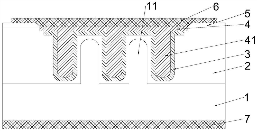
[0034] Such as figure 1 As shown, a hyperabrupt varactor diode, including: N-type heavily doped substrate 1, N-type lightly doped epitaxial layer 2, N-type doped buffer layer 3, P-type heavily doped layer 4, oxide layer 5 , the front multilayer metal 6 and the back multilayer metal 7; the N-type lightly doped epitaxial layer 2 is arranged on the N-type heavily doped substrate 1, and the N-type doped buffer layer 3 and the P-type heavily doped layer 4 are arranged on the In the upper part of the N-type lightly doped epitaxial layer 2, the N-type doped buffer layer 3 is arranged between the P-type heavily doped layer 4 and the N-type lightly doped epitaxial layer 2, and the oxide layer 5 is arranged on the N-type lightly doped epitaxial layer. On the upper surface of layer 2, the front multilayer metal 6 is arranged above the oxide layer 5 and communicated with the P-type heavily doped layer 4, and the back multilayer metal 7 is arranged under the N-type heavily doped substrate ...

Embodiment 2

[0043] This embodiment provides a method for preparing the hyperabrupt varactor diode as described in Embodiment 1, comprising the following steps:

[0044] Step 1: Forming an N-type heavily doped layer and bump 2 on an N-type heavily doped substrate by photolithography and etching;

[0045] Step 2: forming an N lightly doped epitaxial layer on the N type heavily doped substrate and the N type heavily doped layer;

[0046] Step 3: forming an oxide layer on the N lightly doped epitaxial layer;

[0047] Step 4: forming trenches on the oxide layer by photolithography and etching;

[0048] Step 5: epitaxially forming an N-type doped buffer layer above the trench;

[0049] Step 6: removing excess N-type doped buffer layer by photolithography and etching;

[0050] Step 7: Forming a P-type heavily doped layer by epitaxy above the N-type doped buffer layer and the N lightly doped epitaxial layer;

[0051] Step 8: removing the excess P-type heavily doped layer by etching;

[0052]...


PUM

PropertyMeasurementUnit
heightaaaaaaaaaa
widthaaaaaaaaaa
thicknessaaaaaaaaaa

Abstract

The invention discloses a hyper-mutation variable capacitance diode in the technical field of radio frequency semiconductor devices. The hyper-mutation variable capacitance diode comprises an N-type heavily doped substrate; an N-type lightly doped epitaxial layer which is arranged above the N-type heavily doped substrate; a P-type heavily-doped layer which is arranged on the upper portion in the N-type lightly-doped epitaxial layer, wherein the P-type heavily-doped layer extends downwards to form a plurality of first protrusions, and the first protrusions are columnar and distributed at intervals; and an N-type doped buffer layer which is arranged between the N-type lightly doped epitaxial layer and the P-type heavily doped layer. The sections of the P-type heavily-doped layer and the N-type doped buffer layer extend into the N-type lightly-doped epitaxial layer in an interpolation manner, so that the zero-bias junction capacitance of a device is increased on the premise of not increasing the reverse-bias junction capacitance, and the variable capacitance ratio of the device is remarkably increased.

Description

technical field [0001] The invention relates to the technical field of radio frequency semiconductor devices, in particular to a hyperabrupt varactor diode. Background technique [0002] At present, radio applications have been integrated into all aspects of life, such as radio frequency radio stations, walkie-talkies, and mobile phone communications. Especially in the field of mobile communication, from 2G to 5G, with the gradual increase of mobile phone spectrum, handheld wireless communication devices need to integrate multiple spectrums together, so as to reduce the power consumption of the device, reduce the overall weight of the device and reduce the size of the device the goal of. Using YIG, varactor diodes, MEMS devices, etc. to realize reconfigurable filters is an important way to integrate multiple spectrums. Varactor diodes are favored by more and more practitioners due to their advantages of small size, large frequency adjustment range, and easy integration. ...

Claims


Application Information

Patent Timeline
Patent Type & Authority Applications(China)
IPC IPC(8): H01L29/93H01L29/06
CPCH01L29/93H01L29/0684
Inventor 马文力董文俊张雪飞李浩徐婷
Owner YANGZHOU GUOYU ELECTRONICS
Why Eureka
Try Eureka