

Display substrate, manufacturing method thereof and display device
A technology for a display substrate and a manufacturing method, which is applied in semiconductor/solid-state device manufacturing, electrical components, transistors, etc., and can solve problems such as poor threshold voltage uniformity
- Summary
- Abstract
- Description
- Claims
- Application Information
AI Technical Summary
Problems solved by technology
Method used
Image

Examples
Embodiment 1
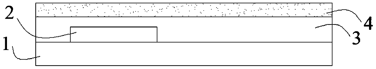
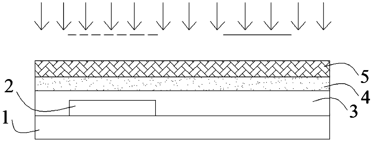
[0046] see Figure 10 and Figure 15 , this embodiment provides a display substrate, including a substrate 1, and a first transistor and a second transistor disposed on the substrate 1, the first transistor and the second transistor are both top-gate thin film transistors, and the first transistor includes a first The active layer 41 and the first gate 71 , the second transistor includes the second active layer 42 and the second gate 72 , the first active layer 41 and the second active layer 42 are oxide semiconductors of the same material.
[0047] The first active layer 41 includes a first portion overlapping with the first grid 71, the second active layer 42 includes a second portion overlapping with the second grid 72, and the orthographic projection of the first portion on the substrate 1 is positioned at the shading position. In the orthographic projection of the layer 2 on the substrate 1 , the orthographic projection of the second part on the substrate 1 does not over...
Embodiment 2
[0057] This embodiment provides a display device, which includes the display substrate of Embodiment 1.
[0058] Specifically, the display device can be any product or component with a display function such as a liquid crystal display panel, an organic light-emitting diode (OLED) display panel, a mobile phone, a tablet computer, a television set, a monitor, a notebook computer, a digital photo frame, and a navigator.
[0059] That is, the above-mentioned first transistor as a driving transistor may drive an electrode of a liquid crystal capacitor, may also drive a cathode or an anode of a light-emitting diode, or drive an electrode of another type of light-emitting device, which is not limited in the present invention.
Embodiment 3
[0061] This embodiment provides a method for manufacturing a display substrate, including:
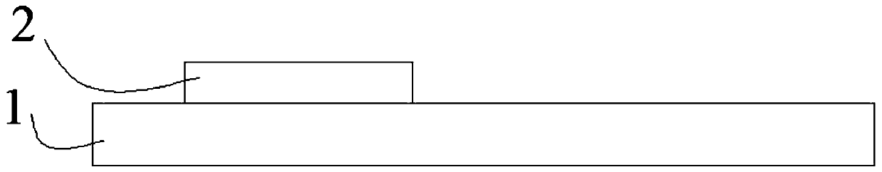
[0062] forming a light-shielding layer 2 on the substrate 1;
[0063] A first transistor is formed, the first transistor is a top-gate thin film transistor, the first transistor includes a first active layer 41 and a first gate 71, the material of the first active layer 41 is an oxide semiconductor, and the first active layer 41 includes a first portion overlapping with the first grid 71, and the orthographic projection of the first portion on the substrate 1 is located within the orthographic projection of the light shielding layer 2 on the substrate 1;
[0064] Forming a second transistor, the second transistor is a top-gate thin film transistor, the second transistor includes a second active layer 42 and a second gate 72, and the material of the second active layer 42 is the same as that of the first active layer 41 an oxide semiconductor, the second active layer 42 includes a seco...
PUM
 Abstract
Description
Claims
Application Information