
Display substrate, display device, and method for manufacturing display substrate

A technology for displaying substrates and manufacturing methods, which is applied in semiconductor/solid-state device manufacturing, semiconductor devices, electrical components, etc., and can solve problems such as poor threshold voltage uniformity

Active Publication Date: 2020-12-01
HEFEI XINSHENG OPTOELECTRONICS TECH CO LTD +1
View PDF6 Cites 0 Cited by
  • Summary
  • Abstract
  • Description
  • Claims
  • Application Information

AI Technical Summary

Problems solved by technology

[0004] The present invention at least partly solves the problem of poor threshold voltage uniformity of top-gate organic oxide semiconductor thin film transistors in existing display substrates, and provides a display substrate, a display device, and a method for manufacturing a display substrate

Method used


Image

  • Display substrate, display device, and method for manufacturing display substrate
  • Display substrate, display device, and method for manufacturing display substrate
  • Display substrate, display device, and method for manufacturing display substrate

Examples


Embodiment 1

[0046] see Figure 10 and Figure 15 , this embodiment provides a display substrate, including a substrate 1, and a first transistor and a second transistor disposed on the substrate 1, the first transistor and the second transistor are both top-gate thin film transistors, and the first transistor includes a first The active layer 41 and the first gate 71 , the second transistor includes the second active layer 42 and the second gate 72 , the first active layer 41 and the second active layer 42 are oxide semiconductors of the same material.

[0047] The first active layer 41 includes a first portion overlapping with the first grid 71, the second active layer 42 includes a second portion overlapping with the second grid 72, and the orthographic projection of the first portion on the substrate 1 is positioned at the shading position. In the orthographic projection of the layer 2 on the substrate 1 , the orthographic projection of the second part on the substrate 1 does not over...

Embodiment 2

[0057] This embodiment provides a display device, which includes the display substrate of Embodiment 1.

[0058] Specifically, the display device can be any product or component with a display function such as a liquid crystal display panel, an organic light-emitting diode (OLED) display panel, a mobile phone, a tablet computer, a television set, a monitor, a notebook computer, a digital photo frame, and a navigator.

[0059] That is, the above-mentioned first transistor as a driving transistor may drive an electrode of a liquid crystal capacitor, may also drive a cathode or an anode of a light-emitting diode, or drive an electrode of another type of light-emitting device, which is not limited in the present invention.

Embodiment 3

[0061] This embodiment provides a method for manufacturing a display substrate, including:

[0062] forming a light-shielding layer 2 on the substrate 1;

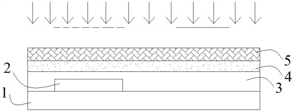
[0063] A first transistor is formed, the first transistor is a top-gate thin film transistor, the first transistor includes a first active layer 41 and a first gate 71, the material of the first active layer 41 is an oxide semiconductor, and the first active layer 41 includes a first portion overlapping with the first grid 71, and the orthographic projection of the first portion on the substrate 1 is located within the orthographic projection of the light shielding layer 2 on the substrate 1;

[0064] Forming a second transistor, the second transistor is a top-gate thin film transistor, the second transistor includes a second active layer 42 and a second gate 72, and the material of the second active layer 42 is the same as that of the first active layer 41 an oxide semiconductor, the second active layer 42 includes a seco...


PUM


Abstract

The invention provides a display substrate, a manufacturing method thereof and a display device, and belongs to the technical field of display; and the problem that a top gate type organic oxygen compound semiconductor film transistor in a present display substrate is low in uniformity of threshold voltage can be solved partially. In the display substrate, a first active layer comprises a first part overlapped with a first gate, a second active layer comprises a second part overlapped with a second gate, an orthographic projection of the first part in the substrate is positioned within an orthographic projection of a light shield layer in the substrate, and an orthographic projection of the second part in the substrate is not overlapped with the orthographic projection of the light shieldlayer in the substrate; and a multiplier of the majority carrier concentration of the first part and the thickness of the first part is lower than that of the concentration of the second part and thethickness of the second part.

Description

technical field [0001] The invention belongs to the field of display technology, and in particular relates to a display substrate, a display device and a manufacturing method of the display substrate. Background technique [0002] For thin film transistors in display substrates, it has been reported that an oxide semiconductor is used as an active layer. Since top-gate thin film transistors have better performance than bottom-gate thin film transistors, such as smaller parasitic capacitance and smaller size, more and more attention has been paid to their application in display substrates. [0003] In the above display substrate, some of the thin film transistors are used as driving transistors, and some of the thin film transistors are used as switching transistors. Relatively speaking, the stability of the characteristics of the driving transistor is required to be higher, so a blocking layer is formed between the driving transistor and the substrate to prevent external li...

Claims


Application Information

Patent Timeline
Patent Type & Authority Patents(China)
IPC IPC(8): H01L27/12H01L29/06H01L29/786H01L21/77
Inventor 宋威赵策丁远奎苏同上刘宁王海涛汪军倪柳松
Owner HEFEI XINSHENG OPTOELECTRONICS TECH CO LTD
Learn More