High-temperature and high-humidity reverse bias test system and method for semiconductor device

A high-temperature, high-humidity, test system technology, applied in the direction of single semiconductor device testing, etc., can solve the problem of high cost, achieve the effect of reducing test cost, reducing test space, and improving batch test efficiency

Active Publication Date: 2019-05-17
CHONGQING PINGWEI ENTERPRISE
View PDF5 Cites 4 Cited by
  • Summary
  • Abstract
  • Description
  • Claims
  • Application Information

AI Technical Summary

Problems solved by technology

In the existing test system and test device, in the environment of high temperature and high humidity, it is necessary to configure expensive special fuses, and the cost is high

Method used


Image

  • High-temperature and high-humidity reverse bias test system and method for semiconductor device
  • High-temperature and high-humidity reverse bias test system and method for semiconductor device
  • High-temperature and high-humidity reverse bias test system and method for semiconductor device

Examples


Embodiment Construction

[0038] In the following description, numerous specific details are given in order to provide a more thorough understanding of the present invention. It will be apparent, however, to one skilled in the art that the present invention may be practiced without one or more of these details. In other examples, some technical features known in the art are not described in order to avoid confusion with the present invention.

[0039] It should be understood that the invention can be embodied in different forms and should not be construed as limited to the embodiments set forth herein. Rather, these embodiments are provided so that this disclosure will be thorough and complete, and will fully convey the scope of the invention to those skilled in the art. In the drawings, like reference numerals refer to like components throughout.

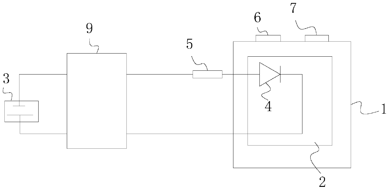
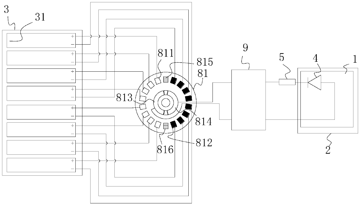
[0040] The semiconductor device and the semiconductor device to be tested in the following embodiments may be diodes or MOSFETs.

[0041] A kind of high...


PUM


Abstract

The invention provides a high-temperature and high-humidity reverse bias test system and method for a semiconductor device. In the test system and the test method, a protective tube is arranged outside a test box; the special protective tube can be replaced by an ordinary protective tube; therefore, the test cost is easily reduced; furthermore, a test space occupied by the protective tube in the text box is reduced; therefore, more test stations can be easily provided in the test box; and the batch test efficiency is increased.

Description

technical field [0001] The invention relates to the field of semiconductor device tests, in particular to a high-temperature, high-humidity reverse bias test system and test method for semiconductor devices. Background technique [0002] The aging test of semiconductor devices is an important means to control the quality of semiconductor devices. When using the existing aging test standards (see standard AECQ101) to conduct reverse bias tests on semiconductor devices such as diodes or MOSFETs, the maximum reverse bias voltage loaded is 100V; However, in practical applications, the reverse voltage threshold that semiconductor devices can withstand is likely to be much greater than 100V. For example, in the automotive field, some semiconductor devices need not be damaged when the reverse bias voltage reaches 800V. According to the application scenario, some The application environment of semiconductor devices is harsh. Therefore, during the aging test, it is necessary to simul...

Claims


Application Information

Patent Timeline
Patent Type & Authority Applications(China)
IPC IPC(8): G01R31/26
Inventor 张兴武易明军王兴龙陈苗
Owner CHONGQING PINGWEI ENTERPRISE
Why Eureka
Try Eureka