bridging device for an AHB bus to access an on-chip SRAM

A bridging device and bus technology, applied in the field of high-speed data processing, can solve the problems of read operation delay, affecting system efficiency, etc., and achieve the effect of optimizing the timing of reading and writing

Active Publication Date: 2019-05-24
ZHEJIANG UNIV
View PDF5 Cites 4 Cited by
  • Summary
  • Abstract
  • Description
  • Claims
  • Application Information

AI Technical Summary

Problems solved by technology

Therefore, the disadvantage of this commonly used bridge device is that the read operation initiated by the AHB host will be delayed, which seriously affects the efficiency of the system operation.

Method used


Image

  • bridging device for an AHB bus to access an on-chip SRAM
  • bridging device for an AHB bus to access an on-chip SRAM
  • bridging device for an AHB bus to access an on-chip SRAM

Examples


Embodiment Construction

[0028] The technical solution of the present invention will be further described below in conjunction with the accompanying drawings of the description.

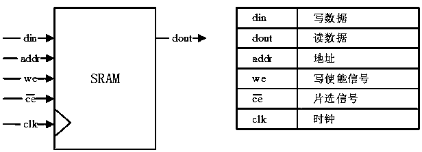
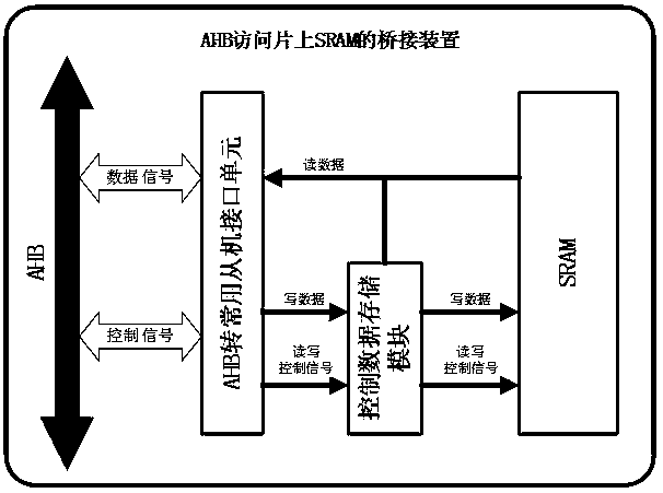
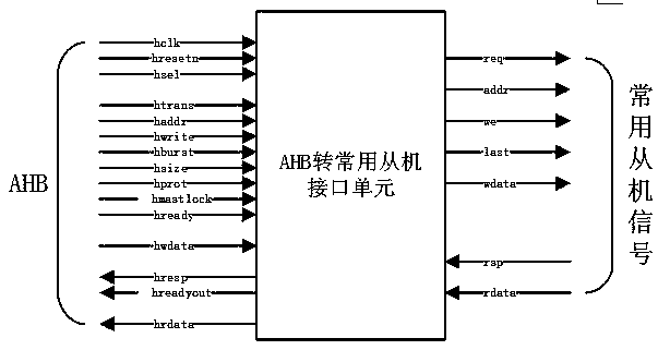
[0029] The bridge device for AHB accessing on-chip SRAM proposed in this patent is as follows: figure 2 As shown, it mainly includes two modules: one module is an AHB-to-common slave interface unit, and the other module is a control data storage module. Depend on figure 2 It can be seen that the AHB signal is converted into a common slave interface signal after being processed by the AHB to common slave interface unit and connected to the control data storage module and SRAM. SRAM signals such as figure 1 As shown, the write data and control signals in the commonly used slave interface unit need to be processed by the control data storage module before the signal can be transmitted to the SRAM; the read data in the commonly used slave interface unit can be obtained from the SRAM or from the control data storage module. ...


PUM


Abstract

The invention discloses a bridging device for an AHB bus to access an on-chip SRAM, and belongs to the field of data high-speed processing in SoC design. The bridging device comprises an AHB-to-commonslave interface unit and a control data storage module; the AHB-to-common slave interface unit converts an AHB signal into a common slave interface signal and is connected with the control data storage module and the SRAM; And the control data storage module registers the control signal and the data signal of the write operation, transmits the control signal and the data signal to the SRAM, and processes the signal read after writing. When the condition of reading after writing occurs; Through the processing of the bridging device, the read operation is preferentially ensured not to be blocked, the data of the write operation and the control signal are temporarily cached in the register, so that the situation that the SRAM is accessed while reading and writing is avoided, and meanwhile, the time sequence efficiency of the system is greatly improved due to the fact that the read data can be timely transmitted to the host.

Description

technical field [0001] The invention relates to the field of high-speed data processing in SoC design, in particular to a bridge device for AHB bus accessing on-chip SRAM. Background technique [0002] System on Chip (SoC, System on Chip), also known as system on chip, as the name implies, integrates a complete system on a single chip. System chips are mainly used in embedded systems, mobile devices, personal computers and other fields. The hardware functional units required for a complete system chip mainly include processor cores, storage devices (Memories), input and output interfaces (Interfaces), IP cores, etc., and sometimes DSP (Digital Signal Processor, digital signal processor) and other A functional unit that implements a special application. SoCs have two notable features: First, in order to complete the functions of the entire system, many functional units are often required, so the scale of hardware is huge, so SoCs often adopt an IP-based design model. Secon...

Claims


Application Information

Patent Timeline
Patent Type & Authority Applications(China)
IPC IPC(8): G06F13/28G06F13/40
Inventor 黄凯陈子旋余慜修思文
Owner ZHEJIANG UNIV
Why Eureka
Try Eureka