A driving circuit of a display panel and an image display device

A driving circuit and display panel technology, applied to static indicators, instruments, etc., can solve the problem of large driving circuit area, achieve simple structure, good display uniformity, and reduce the chip area.

Inactive Publication Date: 2019-05-28
SEEYA OPTRONICS LTD
View PDF5 Cites 0 Cited by
  • Summary
  • Abstract
  • Description
  • Claims
  • Application Information

AI Technical Summary

Problems solved by technology

Since the data voltage output by each DAC corresponds to a pixel circuit, a group of DACs is required, so the area in the driving circuit is very large

Method used


Image

  • A driving circuit of a display panel and an image display device
  • A driving circuit of a display panel and an image display device
  • A driving circuit of a display panel and an image display device

Examples


Embodiment 1

[0045] image 3 It is a schematic circuit structure diagram of a driving circuit of a display panel according to an embodiment of the present invention.

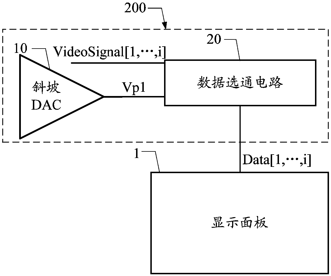
[0046] The driving circuit 200 of the display panel 1 in this embodiment may include a ramp DAC10 and a data gating circuit (not shown in the figure). For more information about the ramp DAC10 and the data strobe circuit, see the previous article on figure 2 The related description of the driving circuit 200 shown will not be repeated here.

[0047] In this embodiment, M=N, for example, the number of digits of the slope DAC10 and each digital video signal VideoSignal[1,...,i] is equal to 8, but not limited thereto, M and N can be any other suitable positive integer.

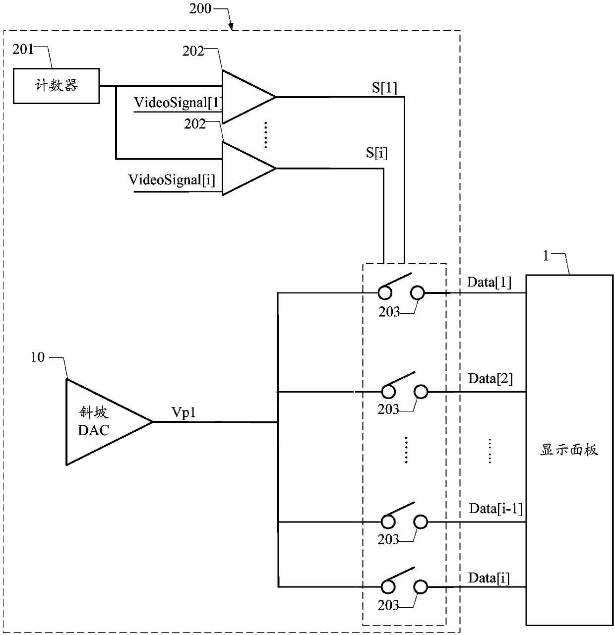
[0048] Preferably, the first slope voltage Vp1 changes linearly and incrementally. The data gating circuit may include a counter 201 , i value comparators 202 and i first switches 203 .

[0049]Wherein, the i value comparators 202 are adapted to respectiv...

Embodiment 2

[0056] Figure 4 It is a schematic circuit structure diagram of another driving circuit of the display panel 1 according to the embodiment of the present invention.

[0057] Figure 4 The shown driving circuit 300 of the display panel 1 may include a ramp DAC10 and a data gating circuit (not shown in the figure). For more information about the ramp DAC10 and the data strobe circuit, see the previous article on figure 2 The related description of the driving circuit 200 shown will not be repeated here.

[0058] In this embodiment, M

[0059] Wherein, the first step adjustment module 30 is adapted to adjust the amplitude of the first slope voltage Vp1 to obtain 2 N-M A second ramp voltage Vp2[1,...,2 N-M ], the amplitude of the first second slope voltage Vp2[1] is equal to the first slope voltage Vp1, and the other 2 N-M - 1 second ramp voltage Vp2[2,...,2 N-M ] on the bas...

Embodiment 3

[0078] Figure 5 It is a schematic circuit structure diagram of another driving circuit of the display panel 1 according to the embodiment of the present invention.

[0079] Figure 5 The shown driving circuit 400 of the display panel 1 may include a ramp DAC10 and a data gating circuit (not shown in the figure). For more information about the ramp DAC10 and the data strobe circuit, see the previous article on figure 2 The related description of the driving circuit 200 shown will not be repeated here.

[0080] In this embodiment, M

[0081] Wherein, the i second step adjustment modules 60 are adapted to respectively adjust the amplitude of the first slope voltage Vp1 to obtain the corresponding third slope voltage Vp3[1,...,i], the third slope The amplitude ratio of the voltage Vp3[1,...,i] to the corresponding first slope voltage Vp1 is (1+1 / 2 N-M ×P), P is the value ...


PUM


Abstract

A driving circuit of a display panel and an image display device are disclosed, the driving circuit comprising: a ramp DAC adapted to output a first ramp voltage, the first ramp voltage linearly changing over time in a preset voltage range according to a preset step; a data gating circuit, accessing i digital video signals, the data gating module is suitable for generating a corresponding data gating signal at the moment associated with the numerical value of each digital video signal according to each digital video signal, the data gating signal is used for gating the first ramp voltage to directly or indirectly serve as data voltage, and the data voltage is used for controlling the display state of a pixel circuit in the display panel; wherein the slope DAC is M bits, the number of bitsof each digital video signal is N, M is less than or equal to N, and i, M and N are positive integers. By adopting the technical scheme, the area of the driving circuit of the display panel can be effectively reduced.

Description

technical field [0001] The invention relates to the technical field of image display, in particular to a driving circuit of a display panel and an image display device. Background technique [0002] Compared with conventional Liquid Crystal Display (LCD), Organic Light-Emitting Diode (OLED) has a different light-emitting mechanism, with self-illumination, wide viewing angle, almost infinitely high contrast, low Advantages such as power consumption and extremely high response speed. An OLED display includes an array of elements formed by OLEDs. Compared with LCDs, which are driven by voltage, OLEDs are current-driven devices. Therefore, generally, a driving circuit is provided for each OLED in the array. At least the OLED and the driving circuit can be called OLED pixel circuit. Specifically, the magnitude of the driving current generated by the driving circuit is controlled by using the data voltage, and the driving current is used to drive the OLED to emit light. Wherein...

Claims


Application Information

Patent Timeline
Patent Type & Authority Applications(China)
IPC IPC(8): G09G3/36
Inventor 吴桐钱栋李启
Owner SEEYA OPTRONICS LTD
Why Eureka
Try Eureka