Dual-bus dual-power-tube current-limiting circuit, chip and electronic device

A technology of current-limiting circuits and electronic equipment, applied in the field of circuits, can solve the problems of low reliability and high cost of current-limiting protection, and achieve the effects of cost reduction, reliability improvement, and phase deviation avoidance

Active Publication Date: 2019-05-31
ZHANGZHOU KEHUA ELECTRIC TECH CO LTD
10 Cites 0 Cited by

AI-Extracted Technical Summary

Problems solved by technology

[0003] In view of this, the embodiment of the present invention provides a dual-bus dual-power tube current-limiting circuit, chip and electronic equipment to sol...

Method used

The double-busbar dual-power transistor current-limiting circuit that the embodiment of the present invention provides, makes the first triode (or the first transistor) controllable voltage regulator) and the second triode (or the second controllable voltage regulator) are turned on, and then the third triode is turned on, thereby inputting a high-level signal to the feedback signal input terminal of the controller, This enables the controller to achieve current limiting protection for two externally connected power transistors by controlling the duty cycle of the rectangular wave drive signal output by the controller. Since the power resistor is used instead of the transformer to detect the conduction state of the power tube, the cost of the dual-bus dual-power tube current-limiting circuit provided by the embodiment of the present invention is significantly reduced, and the phase deviation between the transformer and the resistance sampling is avoided. , thus improving the reliability of the current limiting protection.
When the current-limited power tube Q5 is turned on, a voltage drop V2 will be generated on the second power resistor R2, and when the V2 voltage is greater than the base-emitter voltage Vbe of the sec...

Abstract

The invention belongs to the technical field of circuits and provides a dual-bus dual-power-tube current-limiting circuit, a chip and an electronic device. The dual-bus dual-power-tube current-limiting circuit comprises a first power resistor, a second power resistor, a pull-up resistor, a first triode, a second triode, a third triode, and a controller. According to the dual-bus dual-power-tube current-limiting circuit, the chip and the electronic device provided by the embodiment of the invention, by means of the voltage drops generated by the two power resistors when the two external power tubes are turned on, the first triode or the second triode is turned on such that the third triode is turned on. Thus, a high-level signal is input into the feedback signal input end of the controller,so that the controller, by controlling the duty ratio of a rectangular wave driving signal output by itself, achieves current-limiting protection of the two external power tubes.

Application Domain

Emergency protective arrangements for limiting excess voltage/current

Technology Topic

Pull-up resistorCurrent limiting +8

Image

  • Dual-bus dual-power-tube current-limiting circuit, chip and electronic device
  • Dual-bus dual-power-tube current-limiting circuit, chip and electronic device
  • Dual-bus dual-power-tube current-limiting circuit, chip and electronic device

Examples

  • Experimental program(1)

Example Embodiment

[0028] In the following description, for the purpose of illustration rather than limitation, specific details such as a specific system structure and technology are proposed for a thorough understanding of the embodiments of the present invention. However, it should be clear to those skilled in the art that the present invention can also be implemented in other embodiments without these specific details. In other cases, detailed descriptions of well-known systems, devices, circuits, and methods are omitted to avoid unnecessary details from obstructing the description of the present invention.
[0029] In order to illustrate the technical solution of the present invention, specific embodiments are used for description below.
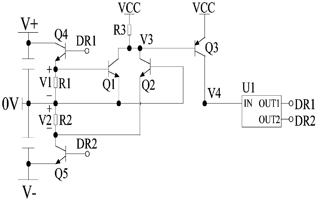
[0030] The embodiment of the present invention provides a dual busbar dual power tube current limiting circuit, such as figure 1 As shown, the dual-bus dual-power tube current limiting circuit may include a first power resistor R1, a second power resistor R2, a pull-up resistor R3, a first transistor Q1, a second transistor Q2, and a third transistor. Q3 and controller U1.
[0031] Specifically, the first end of the first power resistor R1 is connected to the current-limited power tube Q4, and the second end of the first current-limiting resistor R1 is connected to the reference potential 0V. The connection point between the first power resistor R1 and the current-limited power tube Q4, that is, the first end of the first power resistor R1 is also connected to the base of the first transistor Q1, and the emitter of the first transistor Q1 is connected to the Reference potential connection.
[0032] The first end of the second power resistor R2 is connected to another current-limited power tube Q5, and the second end of the second current-limiting resistor R2 is connected to the reference potential 0V. The connection point between the second power resistor R2 and the other current-limited power tube Q5, that is, the first end of the second power resistor R2 is also connected to the emitter of the second transistor Q2, and the base of the second transistor Q2 The pole is connected to the reference potential 0V.
[0033] The first end of the pull-up resistor R3 is connected to the DC power supply VCC, and the second end of the pull-up resistor R3 is respectively connected to the collector of the first transistor Q1 and the collector of the second transistor Q2. The second end of the pull-up resistor R3 is also connected to the base of the third transistor Q3, the emitter of the third transistor Q3 is connected to the DC power supply VCC, and the collector of the third transistor Q3 is connected to the controller U1. The feedback signal input terminal IN is connected.
[0034] When the current-limited power transistor Q4 is turned on, a voltage drop V1 will be generated on the first power resistor R1. When the voltage of V1 is greater than the base-emitter voltage V of the first transistor Q1 be When the first transistor Q1 is turned on, the potential V3 is pulled down, so that the third transistor Q3 is turned on, and the potential V4 gets a high voltage and feeds it back to the controller U1, so that the two output terminals of the controller U1 OUT1 and OUT2 output two rectangular wave drive signals DR1 and DR2, respectively. The two rectangular wave driving signals DR1 and DR2 are used to drive the current-limited power tubes Q4 and Q5, respectively.
[0035] When the current-limited power transistor Q5 is turned on, a voltage drop V2 will be generated on the second power resistor R2. When the voltage of V2 is greater than the base-emitter voltage V of the second transistor Q2 be When the second transistor Q2 is turned on, the potential V3 is pulled down, so that the third transistor Q3 is turned on, and the potential V4 gets a high voltage and feeds it back to the controller U1, so that the two output terminals of the controller U1 OUT1 and OUT2 output two rectangular wave drive signals DR1 and DR2, respectively. The two rectangular wave driving signals DR1 and DR2 are used to drive the current-limited power tubes Q4 and Q5, respectively. The controller U1 can realize current limiting protection for the power tubes Q4 and Q5 by outputting driving signals DR1 and DR2 with different duty cycles.
[0036] figure 1 The transistors Q1 and Q2 are used as switching devices in the MOSFET, but the transistors are easily affected by temperature, so that their conduction voltage drop changes. In order to avoid temperature influence, in a specific embodiment, such as figure 2 As shown, controllable regulators Z1 and Z2 can be used to replace transistors Q1 and Q2, respectively. in figure 2 In, the control terminal of the first controllable voltage stabilizer Z1 is connected to the connection point of the first power resistor R1 and the current-limited power tube Q4, the anode of the first controllable voltage stabilizer Z1 is connected to the reference potential 0V, and the first The cathode of the controllable voltage stabilizer Z1 is connected to the DC power supply VCC via the pull-up resistor R3. The control terminal of the second controllable voltage stabilizer Z2 is connected to the reference potential 0V, the anode of the second controllable voltage stabilizer Z2 is connected to the connection point of the second power resistor R2 and the current-limited power tube Q5, the second controllable The cathode of the voltage stabilizer Z2 is connected to the DC power supply VCC via the pull-up resistor R3. In practical applications, you can choose TL431 controllable precision voltage source as figure 2 The controllable voltage regulators Z1 and Z2.
[0037] The dual busbar dual power tube current limiting circuit provided by the embodiment of the present invention makes the first triode (or first controllable and stable) the voltage drop generated by the two power resistors when the two current limited power tubes are turned on. Voltage regulator) and the second triode (or the second controllable voltage regulator) are turned on, and then the third triode is turned on, thereby inputting a high level signal to the feedback signal input terminal of the controller, so that the controller By controlling the duty ratio of the rectangular wave drive signal output, the current limiting protection for two external power tubes is achieved. The use of power resistors instead of transformers to achieve the detection of the conduction state of the power tubes makes the cost of the dual bus dual power tube current limiting circuit provided by the embodiments of the present invention significantly reduced, and avoids the phase deviation between the transformer and the resistance sampling , Thereby improving the reliability of current limiting protection.
[0038] The embodiment of the present invention also provides another dual busbar dual power tube current limiting circuit, such as image 3 As shown, the dual busbar dual power tube current limiting circuit includes figure 1 In order to avoid repetition, all the components in the current-limiting circuit of the dual-bus and dual-power tube shown are not repeated here. versus figure 1 Compared with the dual busbar dual power tube current limiting circuit shown, image 3 The current limiting circuit of the dual busbar dual power tube shown also includes a first current limiting resistor R4. In a specific embodiment, one end of the first current limiting resistor R4 is connected to the connection point of the first power resistor R1 and the power tube Q4, and the other end of the first current limiting resistor R4 is connected to the base of the first transistor Q1 . Similarly, refer to image 3 , You can also figure 1 and figure 2 A first current-limiting resistor R4 is added to the corresponding position in.
[0039] Optional, such as image 3 As shown, the dual busbar dual power tube current limiting circuit may also include a second current limiting resistor R5. In a specific embodiment, one end of the second current limiting resistor R5 is connected to the reference potential of 0V, and the other end of the second current limiting resistor R5 is connected to the base of the second transistor Q2. Similarly, refer to image 3 , You can also figure 1 and figure 2 A second current limiting resistor R5 is added to the corresponding position in.
[0040] Optional, such as image 3 As shown, the dual busbar dual power tube current limiting circuit may also include a third current limiting resistor R6. In a specific embodiment, one end of the third current limiting resistor R6 is connected to the DC power supply VCC via a pull-up resistor R3, and the other end of the third current limiting resistor R3 is connected to the base of the third transistor Q3. Similarly, refer to image 3 , You can also figure 1 and figure 2 A third current-limiting resistor R6 is added to the corresponding position in.
[0041] Optional, such as image 3 As shown, the dual-bus dual-power tube current limiting circuit may further include a fourth current limiting resistor R7. In a specific embodiment, one end of the fourth current limiting resistor R7 is connected to the collector of the third transistor Q3, and the other end of the fourth current limiting resistor R7 is connected to the feedback signal input terminal IN of the controller U1. Similarly, refer to image 3 , You can also figure 1 and figure 2 A fourth current limiting resistor R7 is added to the corresponding position in.
[0042] Optional, such as image 3 As shown, the dual-bus dual-power tube current limiting circuit may also include a pull-down resistor R8. In a specific embodiment, one end of the pull-down resistor R8 is connected to the feedback signal input terminal IN of the controller U1, and the other end of the pull-down resistor R8 is connected to the reference potential 0V. The fourth current-limiting resistor R7 is used in conjunction with the pull-down resistor R8 to simultaneously realize the input current-limiting and voltage-limiting protection of the controller U1.
[0043] The embodiment of the present invention also provides a chip, such as Figure 4 As shown, the chip 200 includes figure 1 , figure 2 or image 3 The dual busbar dual power tube current limiting circuit 100 is shown. In the chip 200, the dual-bus dual-power tube current limiting circuit 100 can be used for current limiting protection of the power tubes in the chip 200.
[0044] The embodiment of the present invention also provides an electronic device, such as Figure 5 As shown, the electronic device 300 includes figure 1 , figure 2 or image 3 The dual busbar dual power tube current limiting circuit 100 is shown. In the electronic device 300, the dual busbar dual power tube current limiting circuit 100 can be used for current limiting protection of power tubes in the electronic device 300.
[0045] The embodiment of the present invention also provides another electronic device, such as Image 6 As shown, the electronic device 300 includes Figure 4 The chip 200 shown. Since the chip 200 contains such figure 1 , figure 2 or image 3 The dual bus and dual power tube current limiting circuit 100 is shown. Therefore, in the electronic device 300, the chip 200 and the dual bus and dual power tube current limiting circuit 100 contained therein can be used for current limiting protection of the power tube in the electronic device 300.
[0046] The above-mentioned embodiments are only used to illustrate the technical solutions of the present invention, not to limit them; although the present invention has been described in detail with reference to the foregoing embodiments, those of ordinary skill in the art should understand that it can still implement the foregoing The technical solutions recorded in the examples are modified, or some of the technical features are equivalently replaced; these modifications or replacements do not cause the essence of the corresponding technical solutions to deviate from the spirit and scope of the technical solutions of the embodiments of the present invention, and should be included in Within the protection scope of the present invention.

PUM

no PUM

Description & Claims & Application Information

We can also present the details of the Description, Claims and Application information to help users get a comprehensive understanding of the technical details of the patent, such as background art, summary of invention, brief description of drawings, description of embodiments, and other original content. On the other hand, users can also determine the specific scope of protection of the technology through the list of claims; as well as understand the changes in the life cycle of the technology with the presentation of the patent timeline. Login to view more.

Similar technology patents

Apparatus and method for low-density cellular wood plastic composites

InactiveUS20050067729A1less-expensivelow cost
Owner:STRANDEX CORP

Haptic trackball device

InactiveUS7710399B2simple actuatorlow cost
Owner:IMMERSION CORPORATION

Steering Arrangement for a Trailer

InactiveUS20110018231A1low cost
Owner:ZF FRIEDRICHSHAFEN AG

Efficient ultrasound system for two-dimensional c-scan imaging and related method thereof

ActiveUS20060052697A1minimal costlow cost
Owner:UNIV OF VIRGINIA ALUMNI PATENTS FOUND

Classification and recommendation of technical efficacy words

  • low cost

System and method for transmitting wireless digital service signals via power transmission lines

ActiveUS7929940B1reduce bandwidth requirementlow cost
Owner:NEXTEL COMMUNICATIONS

System and method for determination of position

InactiveUS20090149202A1low costreduce requirement
Owner:STEELE CHRISTIAN

Adaptive antenna optimization network

InactiveUS6961368B2low costminimal space
Owner:ERICSSON INC

Antenna device and method for attaching the same

ActiveUS20150138022A1low costimproved strength characteristic
Owner:NEC CORP
Why Eureka
Try Eureka