

Display apparatus and method for manufacturing same
A technology for a display device and a display area, which is applied in the directions of identification devices, lighting devices, semiconductor/solid-state device manufacturing, etc., can solve the problem of not setting a color conversion layer, etc., so as to suppress the manufacturing cost, reduce the number of separate coating and evaporation times, and reduce the stacking sequence. and high degree of freedom in material selection
- Summary
- Abstract
- Description
- Claims
- Application Information
AI Technical Summary
Problems solved by technology
Method used
Image

Examples
Embodiment approach 1
[0061] based on Figure 1 to Figure 8 One embodiment of the present invention will be described below.
[0062] Next, an organic EL display device will be described as an example of the display device according to the present embodiment.
[0063]
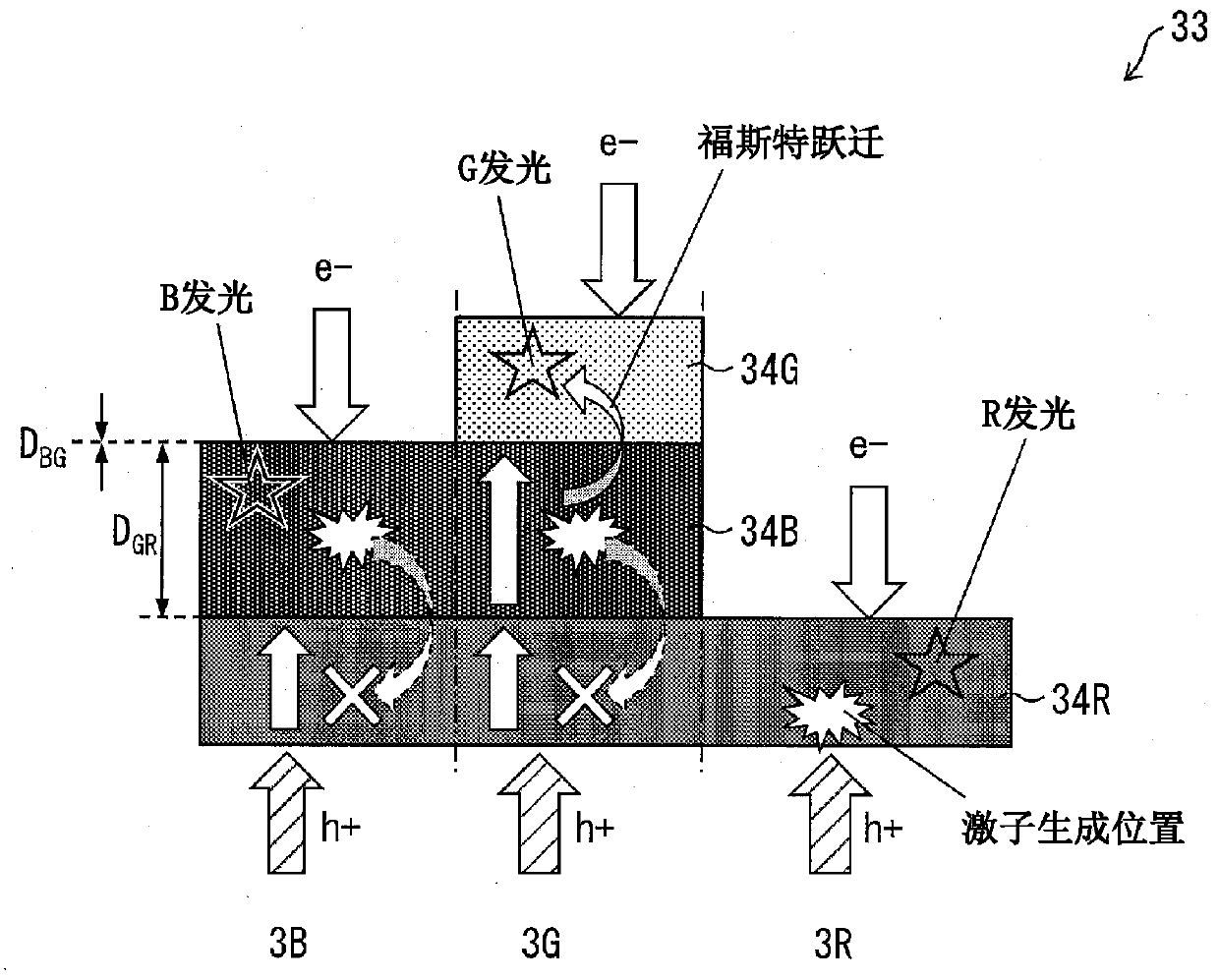
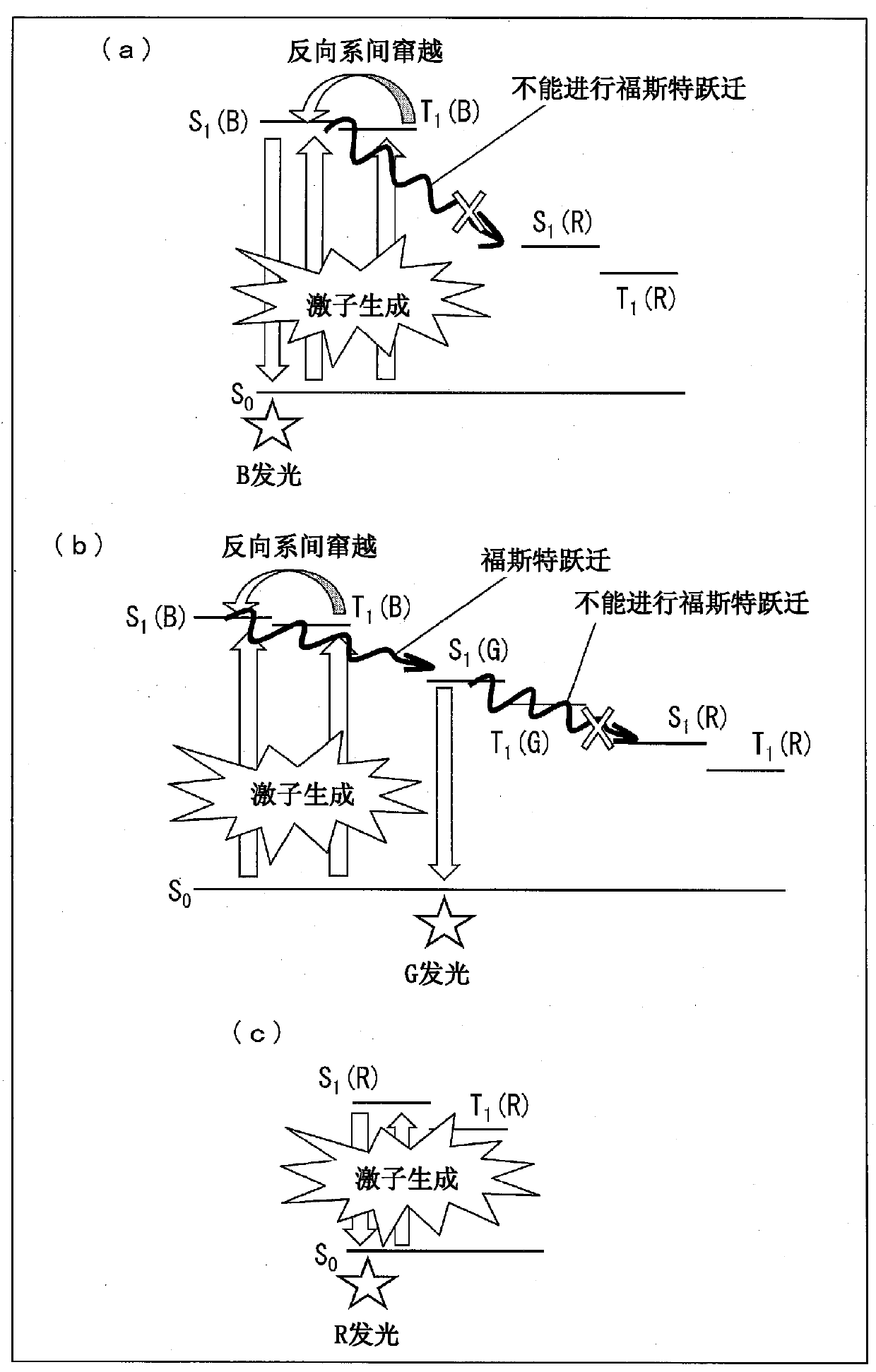
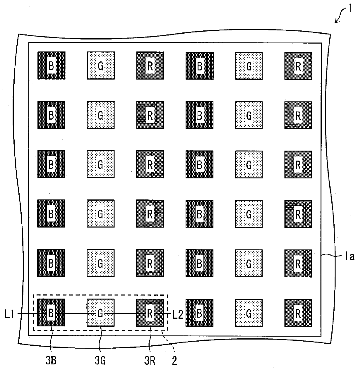
[0064] figure 1 It is a diagram schematically showing the schematic structure of the light-emitting layer unit 33 of the organic EL display device 1 of the present embodiment together with the principle of light emission. figure 2 (a) is a diagram showing the principle of light emission in the sub-pixel 3B of the organic EL display device 1 of this embodiment, figure 2 (b) is a diagram showing the principle of light emission in the sub-pixel 3G of the organic EL display device 1 of this embodiment, figure 2 (c) is a diagram showing the principle of light emission in the sub-pixel 3R of the organic EL display device 1 of the present embodiment. image 3 It is a plan view schematically showing the pixel arrangement of the org...
Embodiment approach 2
[0245] mainly based on Figure 9 (a) to (c) describe another embodiment of the present invention as follows.
[0246] In this embodiment, differences from Embodiment 1 will be described, and components having the same functions as those described in Embodiment 1 will be denoted by the same reference numerals, and description thereof will be omitted. It goes without saying that the same modification as that of Embodiment 1 is possible in this embodiment.
[0247]
[0248] The organic EL display device 1 of the present embodiment has the same configuration as the organic EL display device 1 of the first embodiment except that a red phosphorescent light-emitting material is used as the light-emitting material of the red light-emitting layer 34R. Therefore, the cross-sectional view showing the schematic structure of the organic EL display device 1 of the present embodiment and the Figure 4 same. A cross-sectional view showing a schematic structure of the light-emitting layer...
Embodiment approach 3
[0264] mainly based on Figure 10 Still another embodiment of the present invention will be described below.
[0265] In this embodiment, differences from Embodiments 1 and 2 will be described, and components having the same functions as those described in Embodiments 1 and 2 will be assigned the same reference numerals and descriptions thereof will be omitted. It goes without saying that in this embodiment, the same modifications as in Embodiments 1 and 2 are possible.
[0266]
[0267] Figure 10It is a cross-sectional view showing an example of a schematic configuration of the organic EL display device 1 of the present embodiment. Figure 10 express with image 3 An example of the schematic structure of one pixel region corresponding to the L1-L2 line section of the organic EL display device 1 shown.
[0268] The organic EL display device 1 of the present embodiment is a bottom emission type organic EL display device in which light emitted from the light-emitting laye...
PUM
 Abstract
Description
Claims
Application Information