Pixel defining layer, display substrate, display device, and inkjet printing method

A pixel-defining layer and inkjet printing technology, which is applied in the direction of electrical components, electrical solid devices, circuits, etc., can solve problems such as uneven shape, uneven brightness of pixel areas, affecting the display effect of organic light-emitting display devices, etc., and achieve drying speed Consistent, uniform film effect

Active Publication Date: 2019-06-07
BOE TECH GRP CO LTD +1
View PDF7 Cites 10 Cited by
  • Summary
  • Abstract
  • Description
  • Claims
  • Application Information

AI Technical Summary

Problems solved by technology

Usually, the above-mentioned pixel defining layer has a plurality of openings with different sizes. After using the inkjet printing method to ink-jet print ink in the plurality of openings with different sizes, due to the different volatilization speed of the ink in the openings with different sizes, etc. The shape of the organic light-emitting layer formed in the opening of the organic light-emitting display is often uneven, which leads to uneven brightness of the pixel area of ​​the display device when it emits light, which seriously affects the display effect of the organic light-emitting display device.

Method used


Image

  • Pixel defining layer, display substrate, display device, and inkjet printing method
  • Pixel defining layer, display substrate, display device, and inkjet printing method
  • Pixel defining layer, display substrate, display device, and inkjet printing method

Examples


Embodiment 1

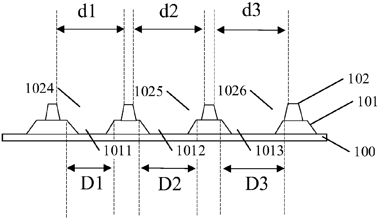
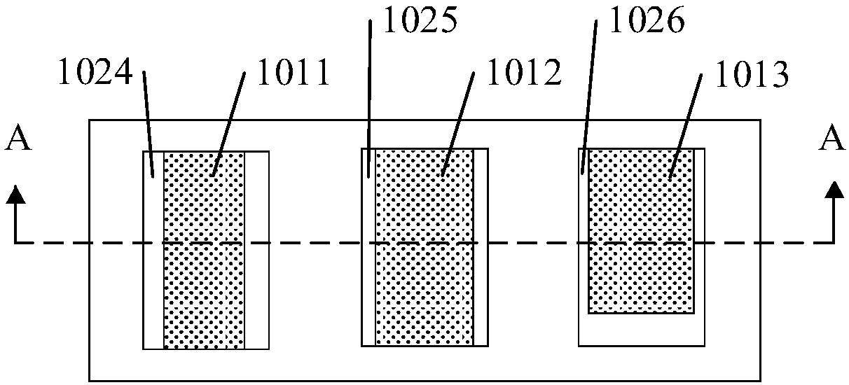
[0042] This embodiment provides a pixel definition layer, figure 1 A schematic cross-sectional view of the pixel defining layer provided in this embodiment, figure 2 A schematic plan view of the pixel defining layer provided in this embodiment, wherein, figure 1 for figure 2 A cross-sectional view of the middle pixel defining layer along the line A-A. Such as figure 1 with figure 2 As shown, the pixel defining layer includes: a first pixel defining layer 101 and a second pixel defining layer 102, the first pixel defining layer 101 has a plurality of first openings with different sizes corresponding to different sub-pixels; the second pixel defining layer 102 is located on the first pixel defining layer 101, and the second pixel defining layer 102 has a plurality of second openings corresponding to different sub-pixels, and the plurality of first openings communicate with the plurality of second openings in one-to-one correspondence, thereby forming corresponding sub-pix...

Embodiment 2

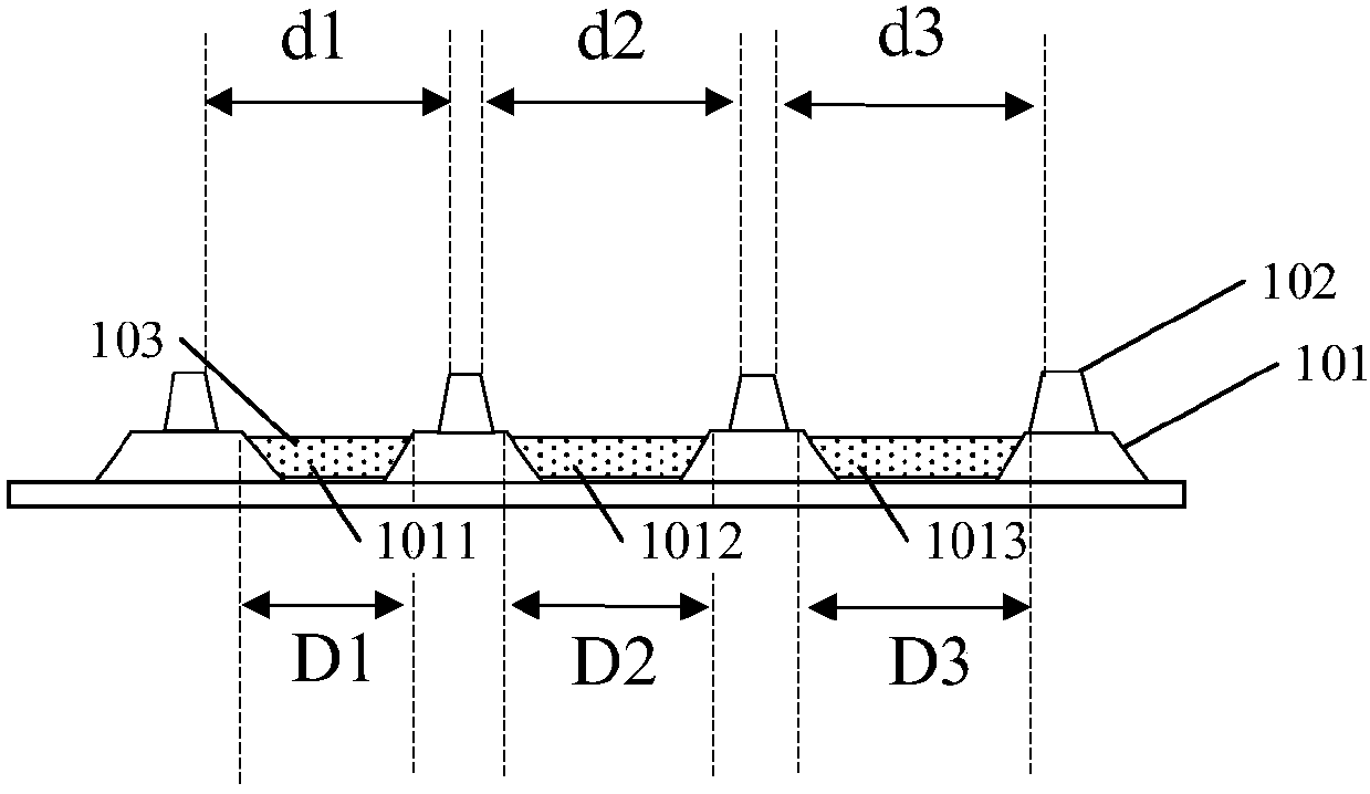
[0063] This embodiment provides an inkjet printing method using any of the above-mentioned pixel defining layers. The pixel defining layer is formed on a base substrate. For example, other structural layers or functional layers are formed on the base substrate. The structural layer is, for example, Including a buffer layer, a passivation layer, etc., the functional layer includes, for example, a driving circuit, etc., and the driving circuit includes devices such as gate lines, data lines, transistors, and capacitors. The pixel defining layer is formed on the above structural layer or functional layer. Such as Figure 3A with Figure 3B As shown, the inkjet printing method includes: performing inkjet printing in the openings provided by the first pixel defining layer 101 and the second pixel defining layer 102 , for example to form the organic functional layer 103 . For example, the height of the ink jet printed in the pixel defining layer is higher than that of the first pi...

Embodiment 3

[0070] This embodiment provides a display substrate, such as Figure 4 As shown, the display substrate includes any one of the above-mentioned pixel defining layers. The pixel defining layer is formed on the base substrate. For example, other structural layers or functional layers are formed on the base substrate. The structural layers include, for example, buffer layers, Passivation layer, etc., the functional layer includes, for example, a driving circuit, etc., and the driving circuit includes gate lines, data lines, transistors, capacitors, and other devices. The pixel defining layer is formed on the above structural layer or functional layer. The display substrate also includes an organic functional layer formed in a plurality of sub-pixel regions obtained by one-to-one communication between the plurality of first openings and the plurality of second openings of the pixel defining layer. The organic functional layer includes a light emitting layer, an electron injection l...


PUM

PropertyMeasurementUnit
Thicknessaaaaaaaaaa
Thicknessaaaaaaaaaa

Abstract

The present invention provides a pixel defining layer, a display substrate, a display device and an inkjet printing method. The pixel defining layer comprises: a first pixel defining layer having a first opening, wherein the first opening comprises a first sub pixel opening and a second sub pixel opening which correspond to different sub pixels, and the size of the opening of the second sub pixelopening is larger than the size of the opening of the first sub pixel opening; and a second pixel defining layer located on the first pixel defining layer, wherein the second pixel defining layer hasa second opening, the second opening has a fourth sub pixel opening corresponding to and communicating with the first sub pixel opening and a fifth sub pixel opening corresponding to and communicatingwith the second sub pixel opening, and the difference of the opening size of the fourth sub pixel opening and the opening size of the first sub pixel opening is larger than the difference of the opening size of the fifth sub pixel opening and the second sub pixel opening. The pixel defining layer is employed for ink jet printing to allow the film layer obtained after ink is dried to be more uniform.

Description

technical field [0001] Embodiments of the present disclosure relate to a pixel defining layer, a display substrate, a display device, and an inkjet printing method. Background technique [0002] Organic light-emitting display devices have the advantages of self-illumination, fast response, wide viewing angle, high brightness, bright colors, light and thin, etc., and thus become an important display technology. [0003] At present, the organic light-emitting layer of an organic light-emitting display device can be formed by inkjet printing, and the formation of the organic light-emitting layer by inkjet printing requires pre-fabricating a pixel defining layer on the substrate to limit the precise injection of ink droplets into the designated area. within the pixel area. Usually, the above-mentioned pixel defining layer has a plurality of openings with different sizes. After using the inkjet printing method to ink-jet print ink in the plurality of openings with different size...

Claims


Application Information

Patent Timeline
IPC IPC(8): H01L27/32H01L51/56
CPCH10K59/352H10K59/122H10K59/173H10K71/135H10K59/353
Inventor 廖金龙
Owner BOE TECH GRP CO LTD
Why Eureka
Try Eureka