A circuit board assembly and electronic equipment

A circuit board assembly, circuit board technology, applied in the field of electronics, can solve problems such as insufficient mechanical connection strength

Active Publication Date: 2020-10-02
VIVO MOBILE COMM CO LTD
View PDF6 Cites 0 Cited by
  • Summary
  • Abstract
  • Description
  • Claims
  • Application Information

AI Technical Summary

Problems solved by technology

[0005] The present invention provides a circuit board assembly and electronic equipment to solve the problem of insufficient mechanical connection strength between various PCBs of the PCB structure in the prior art

Method used


Image

  • A circuit board assembly and electronic equipment
  • A circuit board assembly and electronic equipment
  • A circuit board assembly and electronic equipment

Examples


Embodiment Construction

[0024] In order to make the technical problems, technical solutions and advantages to be solved by the present invention clearer, the following will describe in detail with reference to the drawings and specific embodiments.

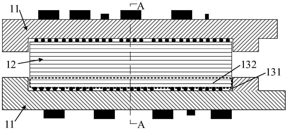
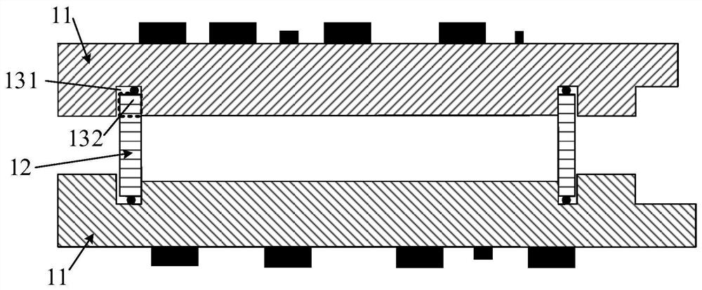
[0025] See Figure 1 to Figure 10 , an embodiment of the present invention provides a circuit board assembly, which may include:

[0026] Two circuit boards 11 arranged oppositely;

[0027] The circuit connection board 12 is arranged between the two circuit boards 11 and connects the two circuit boards 11;

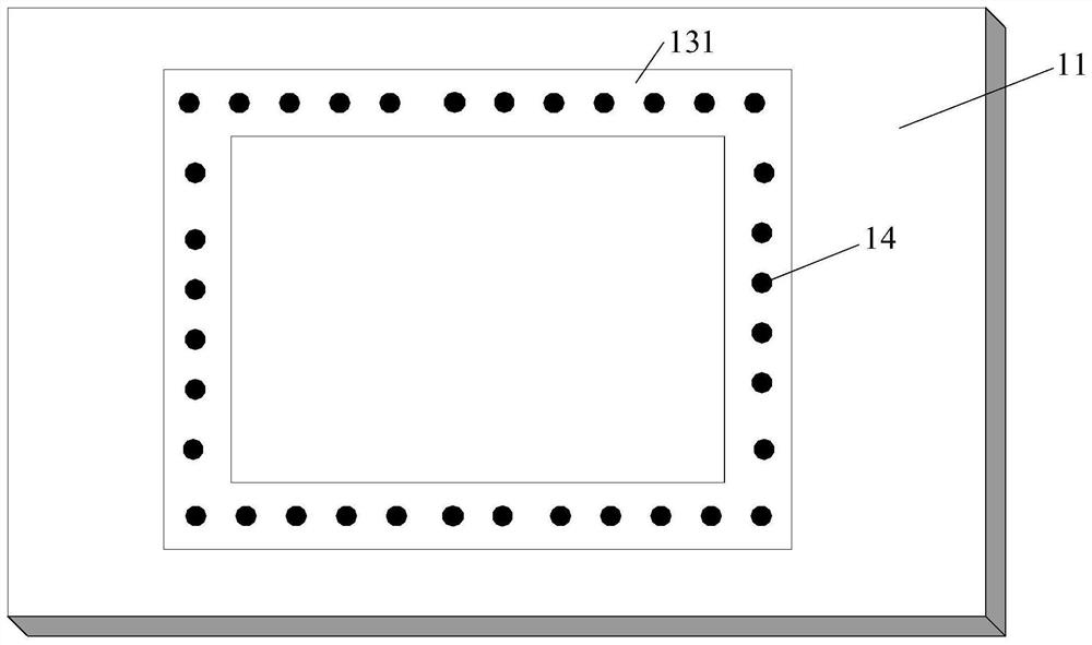
[0028] Wherein, the connecting surface connected with each circuit board 11 on the circuit connecting board 12 is provided with a first snapping structure, and the connecting face connected with the circuit connecting board 12 on the circuit board 11 is provided with a second snapping structure, and the circuit connecting board 12 When connecting with the circuit board 11 , the first engaging structure is matched with the second engaging structure....


PUM


Abstract

The invention provides a circuit board module and electronic equipment. The circuit board module comprises two circuit boards and a circuit connection board, wherein the two circuit boards are arranged opposite to each other, the circuit connection board is arranged between the two circuit boards and is connected with the two circuit boards, a first engagement structure is arranged on a connectionsurface, connected with each circuit board, on the circuit connection board, a second engagement structure is arranged on a connection surface, connected with the circuit connection board, on the circuit board, and the first engagement structure and the second engagement structure are connected in a matching way when the circuit connection board is connected with the circuit boards. The circuit connection board and the circuit boards can be limited and fixed by connection of the first engagement structure and the second engagement structure in a matching way, the displacement quantity of relative motion between the circuit connection board and the circuit boards is limited, and the mechanical connection strength of the circuit board module is improved.

Description

technical field [0001] The invention relates to the field of electronic technology, in particular to a circuit board assembly and electronic equipment. Background technique [0002] With the advent of the 5G era, more and more electronic devices need to be carried on the PCB (Printed Circuit Board, Printed Circuit Board) of electronic devices such as smartphones, and in the limited space, the PCB area is becoming more and more insufficient. [0003] For this reason, some products try to adopt a 3D stacking method, that is, two PCBs are stacked in the thickness direction (Z-axis direction), so as to expand the available area of ​​the PCB by expanding the space in the thickness direction. Usually, this 3D stacking method is vividly called a "sandwich" structure. [0004] However, the above-mentioned "sandwich" structure is relatively fragile in terms of reliability. When the product is subjected to stress impacts such as drop and collision, that is, when the PCB structure is ...

Claims


Application Information

Patent Timeline
Patent Type & Authority Patents(China)
IPC IPC(8): H05K1/14
Inventor 唐后勋付从华
Owner VIVO MOBILE COMM CO LTD
Why Eureka
Try Eureka