Fabrication method of double-sided crimped PCB and PCB
A production method and double-sided technology, applied in the direction of multi-layer circuit manufacturing, electrical connection formation of printed components, etc., can solve the problems of low product yield, difficult operation, complicated process, etc., to improve product yield and simplify the production process , the effect of reducing production costs
- Summary
- Abstract
- Description
- Claims
- Application Information
AI Technical Summary
Problems solved by technology
Method used
Image
Examples
Embodiment 1
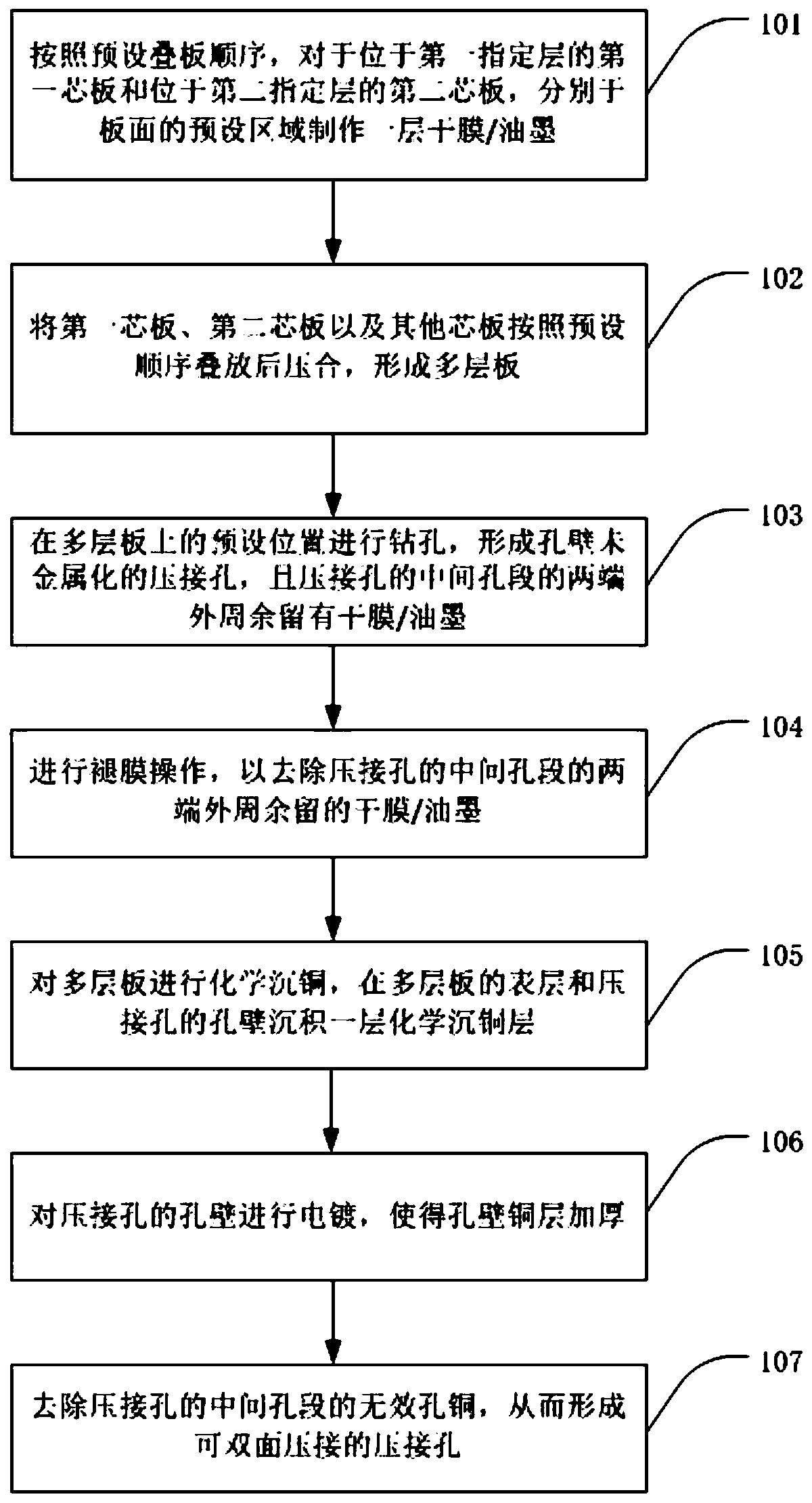
[0049] see figure 1 , the present embodiment provides a method for making a double-sided crimped PCB, comprising steps:
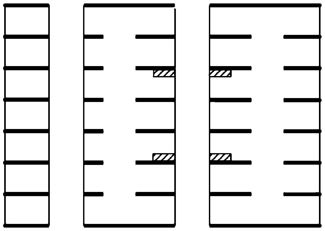
[0050] Step 101, according to the preset stacking sequence, for the first core board located on the first designated layer and the second core board located on the second designated layer, respectively make a layer of dry film / ink on the preset area of the board surface, such as figure 2 shown.
[0051] In this embodiment, according to processing requirements, the crimping hole to be processed can be divided into three hole sections along its axial direction: the upper hole section with metallized hole wall, the middle hole section with unmetallized hole wall and the metallized hole wall. the lower hole section. Based on this, the first specified layer is located at the boundary between the upper hole segment and the middle hole segment, and the second specified layer is located at the boundary between the lower hole segment and the middle hole segment...
Embodiment 2
[0072] see Figure 7 , the present embodiment provides another method for making a double-sided crimped PCB, comprising steps:
[0073] Steps 201 to 203 are the same as steps 101 to 103 in Embodiment 1, and will not be repeated here.
[0074] Step 204 , performing electroless copper deposition on the multilayer board, and depositing a layer of electroless copper deposition on the surface layer of the multilayer board and the hole walls of the crimping holes.
[0075] In this step, a layer of dense thin copper layer with a thickness of 0.1-1.0 microns will be deposited on the hole wall and surface layer through self-catalyzed redox reaction. The copper layer is conductive, so that the hole wall and the surface layer can be connected to facilitate subsequent The hole wall and the surface layer are electroplated with a copper layer at the same time.
[0076] Step 205 , performing a stripping operation to simultaneously remove the dry film / ink and the electroless copper layer on...
Embodiment 3
[0083] On the basis of Embodiment 1 and Embodiment 2, it can further include: making the outer layer circuit pattern; it has two ways of realization: the first is to make the outer layer after removing the invalid hole copper in the middle hole section of the crimping hole Layer circuit pattern, the second is to make the outer layer circuit pattern while removing the invalid hole copper in the middle hole section of the crimping hole.
[0084] The first is to make the outer circuit pattern after removing the invalid hole copper in the middle hole section of the crimping hole, including:
[0085] Step 1. Remove the invalid hole copper in the middle hole section of the crimping hole.
[0086] In this step, there are two ways to remove copper in invalid holes:
[0087] First, the whole board is electroplated to make the surface copper and hole copper thicker; then the whole board is protected by tin plating, so that the board surface and the copper surface of the effective hole ...
PUM
 Abstract
Description
Claims
Application Information


