Organic light emitting display panel, method for manufacturing same, and display device

A technology of light-emitting display and manufacturing method, applied in the direction of semiconductor/solid-state device manufacturing, semiconductor devices, electrical components, etc., can solve the problems affecting the power consumption and life of the display screen, poor uniformity, low transmittance, etc., to prevent natural light interference , Solve the effect of low light absorption rate

Active Publication Date: 2019-06-25
BOE TECH GRP CO LTD +1
View PDF7 Cites 6 Cited by
  • Summary
  • Abstract
  • Description
  • Claims
  • Application Information

AI Technical Summary

Problems solved by technology

[0003] At present, the display screen uses a polarizer plus a 1 / 4 wave plate to improve the interference of external ambient light. This structure can reduce the reflection of the display screen on natural light, and the polarizer will cause the transmittance of the outgoing light from the display screen to be low, which will affect Display Power Consumption and Lifespan
Improving the transmittance of the display screen will improve many problems of the display screen, such as high power consumption, low life, poor uniformity, etc.

Method used


Image

  • Organic light emitting display panel, method for manufacturing same, and display device
  • Organic light emitting display panel, method for manufacturing same, and display device
  • Organic light emitting display panel, method for manufacturing same, and display device

Examples


Embodiment Construction

[0040] The application will be further described in detail below with reference to the drawings and embodiments. It can be understood that the specific embodiments described here are only used to explain the related invention, but not to limit the invention. In addition, it should be noted that, for ease of description, only the parts related to the invention are shown in the drawings.

[0041] It should be noted that the embodiments in the application and the features in the embodiments can be combined with each other if there is no conflict. Hereinafter, the present application will be described in detail with reference to the drawings and in conjunction with embodiments.

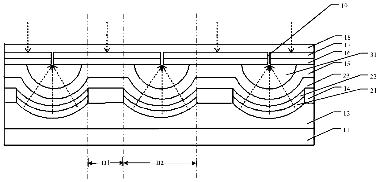
[0042] Please refer to figure 1 , Shows an exemplary structural block diagram of an organic light emitting display panel according to an embodiment of the present application. An organic light emitting display panel includes a substrate, a thin film transistor layer and a flat layer 11. The organic light emi...


PUM


Abstract

The application discloses an organic light emitting display panel, a method for manufacturing the same, and a display device. The organic light emitting display panel comprises a substrate, a thin film transistor layer and a flat layer. The organic light emitting display panel has a non-display area and a display area, and includes a pixel defining layer on the flat layer, wherein the pixel defining layer is provided with a first recess recessed in the thickness direction of the pixel defining layer, a concave curved first electrode layer and a curved light emitting layer are stacked in the first recess, the first electrode layer is adjacent to the pixel defining layer, and the second electrode layer is disposed on the pixel defining layer; an encapsulation layer disposed on the second electrode layer, wherein the encapsulation layer is provided with a second recess recessed in the thickness direction of the encapsulation layer, and the second recess is provided therein with a convex lens; and an anti-interference layer located on the encapsulation layer and provided with a light transmission hole. The light emitted by the curved light emitting layer is condensed by the convex lensand emitted to the outside through the light transmission hole.

Description

Technical field [0001] The present disclosure generally relates to the display field, and in particular, to an organic light-emitting display panel, a manufacturing method thereof, and a display device. Background technique [0002] In the case of strong external ambient light, the display screen reflects part of the natural light, which interferes with the light emitted by the display screen itself. When the external light intensity reflected by the display screen is greater than the light intensity displayed on the display screen itself, the contrast of the display screen will be low and the display effect will decrease. Therefore, reducing the interference of environmental reflected light will greatly improve the display effect of the display under strong light. [0003] At present, the display screen uses a polarizer and a quarter-wave plate to improve the interference of external ambient light. This structure can reduce the reflection of the display screen to natural light, a...

Claims


Application Information

Patent Timeline
Patent Type & Authority Applications(China)
IPC IPC(8): H01L51/50H01L51/52H01L27/32
CPCH10K59/00H10K50/00H10K50/80
Inventor 谢江容夏曾强聂汉
Owner BOE TECH GRP CO LTD
Why Eureka
Try Eureka