
Processing method of luminescent layer of oled panel, oled panel preparation method and oled panel

A processing method and a technology of a light-emitting layer, which are applied in the field of OLED panels, can solve problems such as exciton quenching and uneven thickness of the interface film, and achieve the effects of reducing content, improving interface characteristics, increasing luminous efficiency and lifespan

Active Publication Date: 2021-01-01
SHENZHEN CHINA STAR OPTOELECTRONICS SEMICON DISPLAY TECH CO LTD
View PDF2 Cites 0 Cited by
  • Summary
  • Abstract
  • Description
  • Claims
  • Application Information

AI Technical Summary

Problems solved by technology

However, the light-emitting layer is processed in a solution, and the interface with the evaporated electron transport layer has uneven thickness of the interface, and exciton recombination at the interface leads to exciton quenching and other problems.

Method used


Image

  • Processing method of luminescent layer of oled panel, oled panel preparation method and oled panel

Examples


Embodiment Construction

[0028] The following will clearly and completely describe the technical solutions in the embodiments of the present invention with reference to the accompanying drawings in the embodiments of the present invention. Obviously, the described embodiments are only some, not all, embodiments of the present invention. Based on the embodiments of the present invention, all other embodiments obtained by those skilled in the art without creative efforts fall within the protection scope of the present invention.

[0029] In describing the present invention, it should be understood that the terms "center", "longitudinal", "transverse", "length", "width", "thickness", "upper", "lower", "front", " The orientation or positional relationship indicated by "rear", "left", "right", "vertical", "horizontal", "top", "bottom", "inner", "outer", etc. is based on the orientation shown in the drawings Or positional relationship is only for the convenience of describing the present invention and simpl...


PUM


Abstract

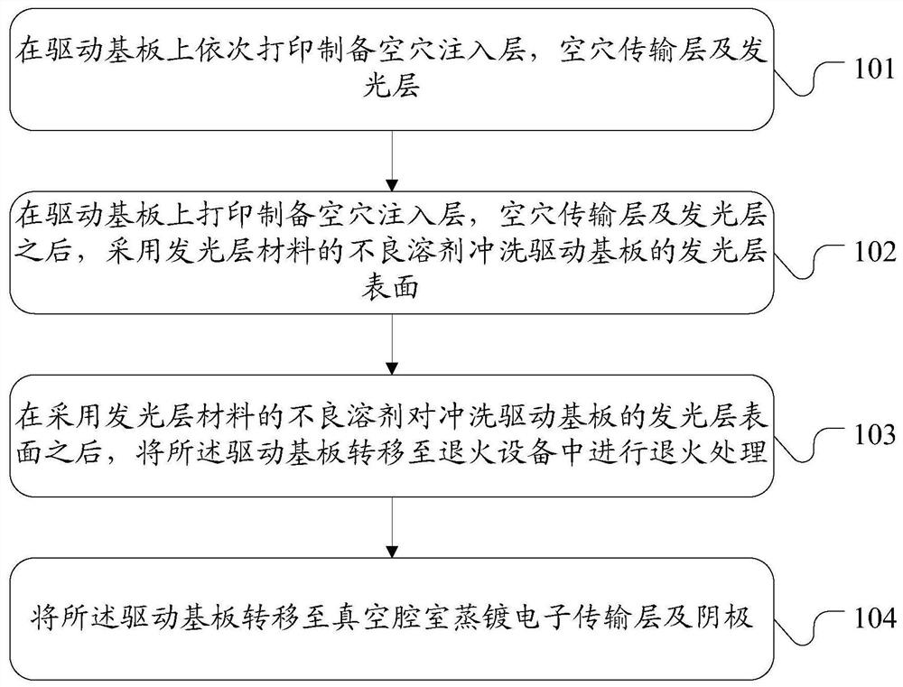
The embodiment of the invention discloses a method for processing the light-emitting layer of an OLED panel, a method for preparing the OLED panel, and the OLED panel. The method for treating the light-emitting layer of the OLED panel includes: after printing and preparing the hole injection layer, the hole transport layer and the light-emitting layer on the driving substrate, the step of washing the surface of the light-emitting layer of the driving substrate with a poor solvent for the material of the light-emitting layer. In the embodiment of the present invention, after the surface of the light-emitting layer of the OLED panel is washed with a poor solvent, the interface characteristics between the later-stage light-emitting layer and the electron transport layer are improved, and the content of doped light-emitting molecules at the interface is reduced, which helps excitons to recombine inside the light-emitting layer, reducing the The probability of recombination and quenching of excitons at the interface is reduced.

Description

technical field [0001] The invention relates to the technical field of semiconductor materials, in particular to a method for processing a light-emitting layer of an OLED panel, a method for preparing an OLED panel, and an OLED panel. Background technique [0002] Organic light-emitting diodes (Organic Light-Emitting Diode, OLED) have been widely used in flat panel display devices due to their advantages such as high contrast, large viewing angle, fast response speed, thinness and flexibility. At present, small-size OLED products adopt vacuum evaporation and fine mask technology to realize RGB (Red, Green, Blue) three-color display, which has become mature. However, large-size OLED products have been abandoned due to the serious warping and deformation of the reticle after the size becomes larger, which increases the difficulty of alignment, resulting in a very low yield. At present, large-size color display is generally realized through white light and color filter technol...

Claims


Application Information

Patent Timeline
Patent Type & Authority Patents(China)
IPC IPC(8): H01L51/56H01L51/50
CPCH10K50/11H10K71/00
Inventor 王士攀
Owner SHENZHEN CHINA STAR OPTOELECTRONICS SEMICON DISPLAY TECH CO LTD
Learn More