Semiconductor element

A semiconductor and component technology, applied in the field of semiconductor components with electrostatic discharge protection function

Inactive Publication Date: 2019-07-26
UPI SEMICON CORP
View PDF0 Cites 0 Cited by
  • Summary
  • Abstract
  • Description
  • Claims
  • Application Information

AI Technical Summary

Problems solved by technology

[0008] In view of this, the present invention provides a semiconductor device to solve the problems mentioned in the prior art

Method used


Image

  • Semiconductor element
  • Semiconductor element
  • Semiconductor element

Examples


Embodiment Construction

[0043] Reference will now be made in detail to the exemplary embodiments of the present invention, examples of which are illustrated in the accompanying drawings. Elements / members with the same or similar numbers used in the drawings and embodiments are used to represent the same or similar parts.

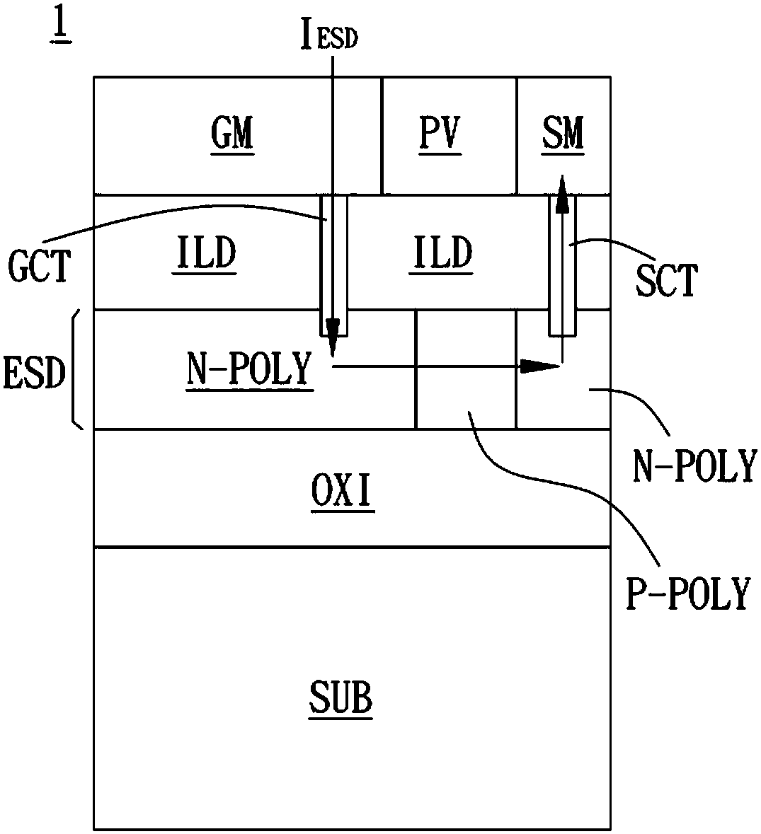
[0044] A preferred embodiment according to the present invention is a semiconductor device. In this embodiment, the semiconductor element may be a metal oxide semiconductor field effect transistor provided with an electrostatic discharge protection element, but it is not limited thereto.

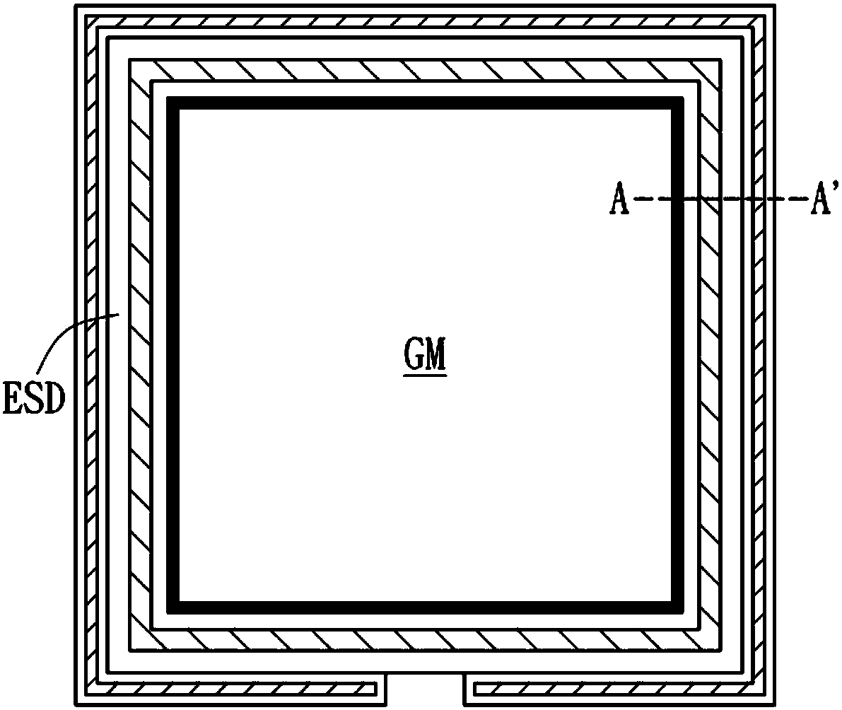
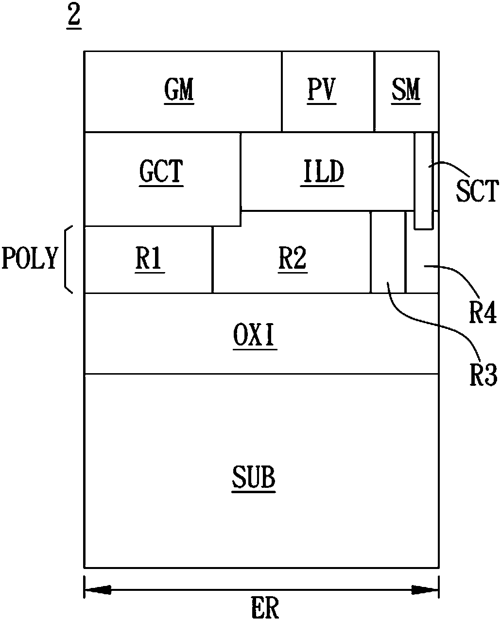
[0045] Please refer to Figure 2A to Figure 2C , Figure 2A A cross-sectional view of a semiconductor element 2 in a preferred embodiment of the present invention is shown; Figure 2B It is a top view of the electrostatic discharge protection polysilicon layer POLY in the semiconductor element 2 including the first doped region R1, the second doped region R2, the third doped region R3 and the ...


PUM


Abstract

The invention provides a semiconductor element with an electrostatic discharge protection function. The semiconductor element comprises a substrate, an electrostatic discharge protection polycrystalline silicon layer, a gate electrode contact part and a source electrode contact part, the substrate defines a gate pad region. An electrostatic discharge protection polysilicon layer is disposed on thesubstrate and in the gate pad region. The electrostatic discharge protection polycrystalline silicon layer comprises a first doped region, a second doped region and a third doped region. The first doped region, the second doped region and the fourth doped region have a first electrical property, and the third doped region has a second electrical property. The second doped region surrounds the first doped region, the third doped region surrounds the second doped region, and the fourth doped region surrounds the third doped region. The doping concentration of the first doped region is higher than that of the second doped region. The gate contact portion is disposed over the first doped region and connects the first doped region and the second doped region. The source electrode contact partis arranged above the fourth doped region and is connected with the fourth doped region. The invention can improve the electrostatic discharge protection capability of the semiconductor element.

Description

technical field [0001] The present invention relates to semiconductor components, in particular to a semiconductor component with electrostatic discharge protection function. Background technique [0002] Known semiconductor elements with electrostatic discharge protection function, taking metal oxide half field effect transistor switching element as an example, the electrostatic discharge protection element is usually arranged around the source or drain with a large area, this configuration will make The ESD current passes through peripheral circuits, resulting in a longer ESD response time and complicating component design. [0003] Therefore, in the prior art, the electrostatic discharge protection element is arranged in the gate pad area of ​​the semiconductor element. The design is relatively simple, but since the gate pad area is relatively smaller than the source / drain pad area, the protection provided by the electrostatic discharge protection device ESD is quite lim...

Claims


Application Information

Patent Timeline
Patent Type & Authority Applications(China)
IPC IPC(8): H01L27/02H01L29/06
CPCH01L27/0248H01L29/0684H01L29/0603
Inventor 蔡政原
Owner UPI SEMICON CORP
Why Eureka
Try Eureka