Active element array substrate
A technology for array substrates and active components, applied in the field of active component array substrates, can solve problems such as decreased protection capabilities, and achieve the effect of reducing mutual interference
- Summary
- Abstract
- Description
- Claims
- Application Information
AI Technical Summary
Problems solved by technology
Method used
Image
Examples
no. 1 example
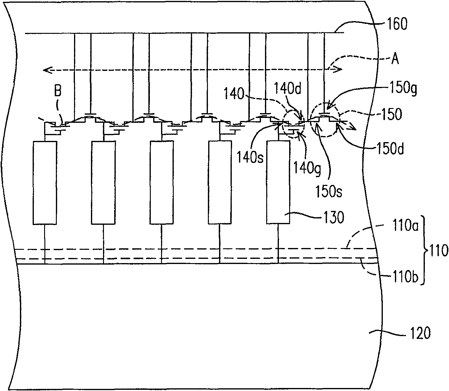
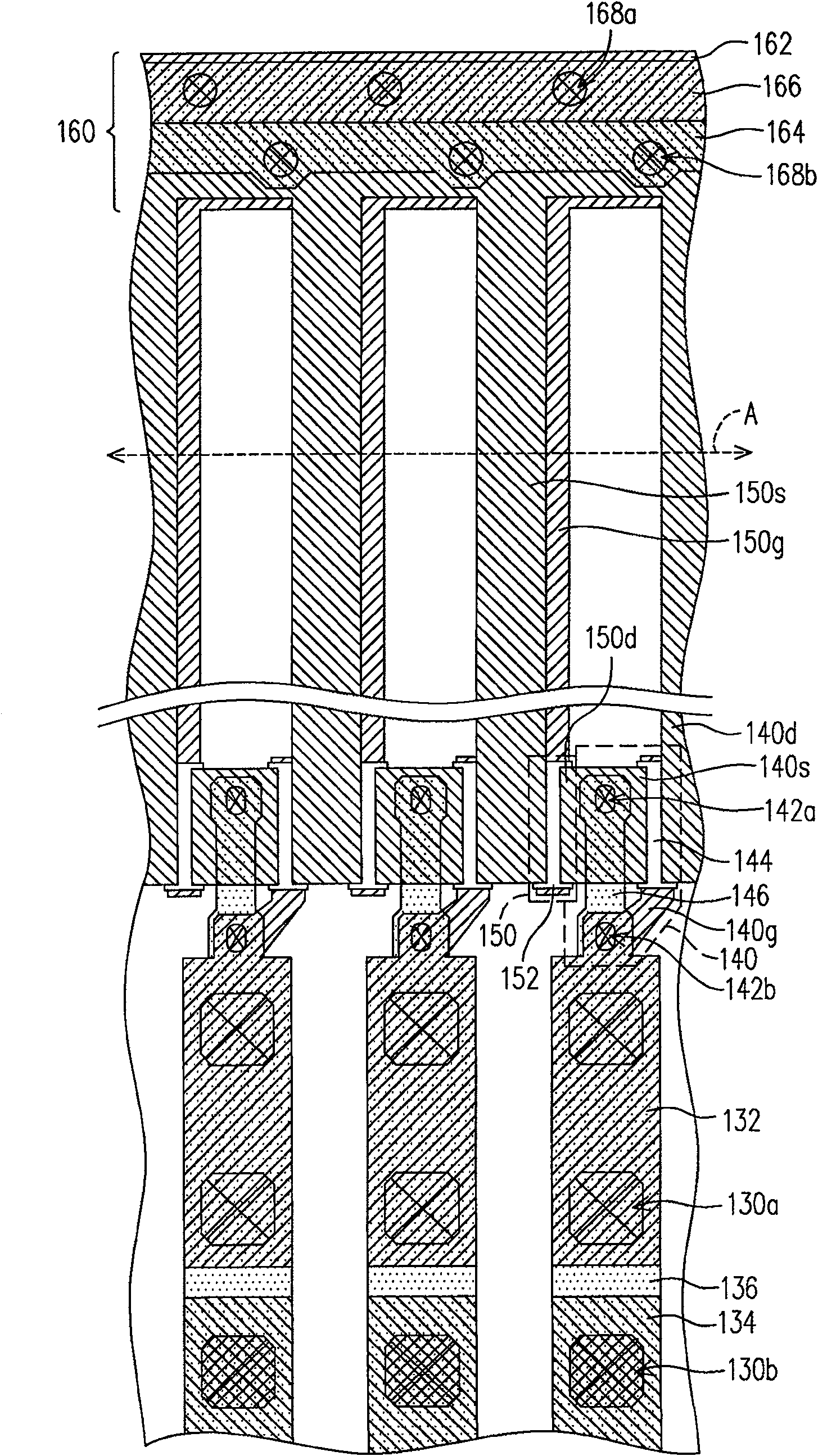
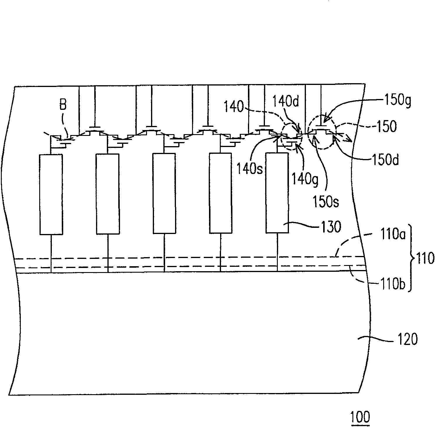
[0040] Figure 1A It is an equivalent circuit diagram of an active element array substrate before cutting process according to the first embodiment of the present invention. Figure 1B It is a top view of an active element array substrate before cutting process according to the first embodiment of the present invention, and the pixel array is not shown.
[0041] Please refer to Figure 1A In this embodiment, the method for manufacturing an active element array substrate includes the following steps. Firstly, a substrate 110 is provided, and the substrate 110 has a peripheral circuit area 110a and a display area 110b, wherein a pixel array 120 has been formed on the display area 110b. The pixel array 120 generally includes a plurality of scan lines, a plurality of data lines, a plurality of thin film transistors, and a plurality of pixel electrodes, but for the sake of simplicity, the detailed structure of the pixel array 120 is not shown. In addition, a plurality of pads 130 ...
no. 2 example
[0051] Figure 3A It is an equivalent circuit diagram of an active element array substrate before cutting process according to the second embodiment of the present invention. Figure 3B It is a top view of an active element array substrate before cutting process according to the second embodiment of the present invention, and the pixel array is not shown. Please refer to Figure 3A , this embodiment is similar to the first embodiment, the difference is that: the gate 250g of each second switching element 250 is electrically connected to the source 250s. Therefore, the second switching element 250 can be regarded as a diode. In addition, the drain 250d of the second switching element 250 is electrically connected to the source 140s of the first switching element 140 .
[0052] The detailed structure will be described in detail below, but it is worth noting that, Figure 3A The structure represented by the equivalent circuit diagram is not limited to Figure 3B The structur...
no. 3 example
[0057] Figure 5A It is an equivalent circuit diagram of an active element array substrate before cutting process according to the third embodiment of the present invention. Figure 5B It is a top view of an active element array substrate before cutting process according to the third embodiment of the present invention, and the pixel array is not shown. Please refer to Figure 5A , this embodiment is similar to the first embodiment, the difference is that: a connection line 370 is also formed on the peripheral circuit area 110a of the substrate 110, which is arranged outside the first switching element 140 and the second switching element 150, And the source 150s of each second switching element 150 is electrically connected to the connection line 370 .
[0058] The detailed structure will be described in detail below, but it is worth noting that, Figure 5A The structure represented by the equivalent circuit diagram is not limited to Figure 5B The structure shown. Those...
PUM
 Abstract
Description
Claims
Application Information


