Method of Separating Flexible Substrate and Rigid Conductive Carrier

A technology of conductive carrier and flexible substrate, applied in the direction of printed circuit, electrical components, multilayer circuit manufacturing, etc., can solve the problems of device failure, increased device cost, performance degradation, etc.

Active Publication Date: 2020-11-06
BEIJING HUATAN TECH CO LTD
View PDF8 Cites 0 Cited by
  • Summary
  • Abstract
  • Description
  • Claims
  • Application Information

AI Technical Summary

Problems solved by technology

Such a process introduces new process steps, increases device cost, and is inefficient
In addition, the upper device is immersed in the corrosive solution, which will easily lead to device failure, performance degradation, and yield reduction
[0005] Although the laser lift-off process is highly efficient, the laser equipment is expensive and has a limited lifespan. Moreover, the process can only be applied to specific opaque flexible PI substrates, and the scope of use is very limited.

Method used


Image

  • Method of Separating Flexible Substrate and Rigid Conductive Carrier
  • Method of Separating Flexible Substrate and Rigid Conductive Carrier

Examples


Embodiment Construction

[0024] The present disclosure will be further described in detail below with reference to the drawings and embodiments. It can be understood that the specific implementation manners described here are only used to explain relevant content, rather than to limit the present disclosure. It should also be noted that, for ease of description, only parts related to the present disclosure are shown in the drawings.

[0025] It should be noted that, in the case of no conflict, the implementation modes and the features in the implementation modes in the present disclosure can be combined with each other. The present disclosure will be described in detail below with reference to the drawings and embodiments.

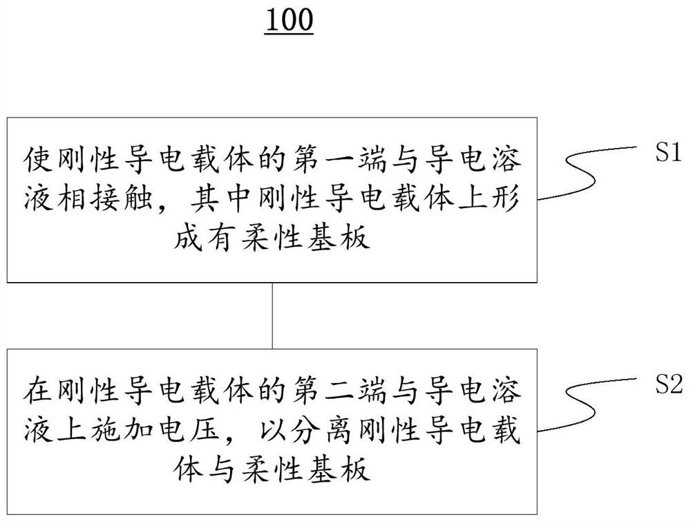
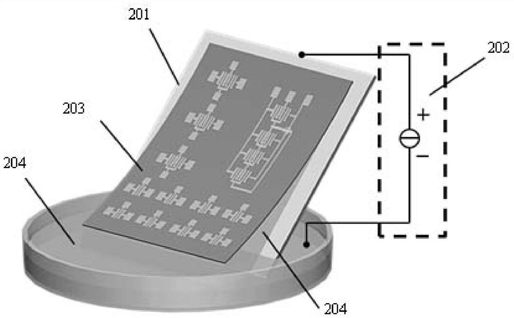
[0026] figure 1 A flowchart of a method of separating a flexible substrate from a rigid conductive carrier according to an embodiment of the present disclosure is shown. like figure 1 As shown, the method 100 of separating a flexible substrate and a rigid conductive carrier ac...


PUM


Abstract

The invention provides a method for separating a flexible substrate and a rigid conductive carrier; the method comprises the following steps that the first end of the rigid conductive carrier is in contact with a conductive solution, wherein the flexible substrate is formed on the rigid conductive carrier; and a voltage is applied to the second end of the rigid conductive carrier and the conductive solution so as to separate the rigid conductive carrier from the flexible substrate, wherein the conductive solution is capable of corroding the surface, facing the flexible substrate, of the rigidconductive carrier.

Description

technical field [0001] The present disclosure relates to flexible substrates, and in particular to a method of separating a flexible substrate from a rigid conductive carrier. Background technique [0002] Flexible electronic devices are electronic or optoelectronic devices that can be bent, folded, or stretched on flexible substrates such as plastics. Flexible electronic devices have shown great application potential in the fields of flexible display, electronic skin, sensing, solar cells, and energy storage. Flexible electronic devices must not only meet high performance standards, but also be able to achieve a more friendly interaction with the human body. This requires that the thickness of flexible electronic devices be reduced to realize thin and light flexible thin film devices. For example, for flexible electronic skin devices to be combined with human skin and other tissues and organs, the overall thickness of the device needs to be greatly reduced to achieve conf...

Claims


Application Information

Patent Timeline
Patent Type & Authority Patents(China)
IPC IPC(8): H05K3/00H05K3/46
CPCH05K3/007H05K3/4682H05K2203/0147H05K2203/10
Inventor 梁世博
Owner BEIJING HUATAN TECH CO LTD
Why Eureka
Try Eureka