Eureka AIR delivers breakthrough ideas for toughest innovation challenges, trusted by R&D personnel around the world.

Electrochromic device and electronic device

A technology of electrochromic devices and electrochromic materials, applied in instruments, nonlinear optics, optics, etc., can solve the problems of ion migration and layering of color-changing materials, and the inability of rapid lateral migration of electrochromic materials. Achieve the effect of avoiding stratification reaction and reducing lateral migration

Active Publication Date: 2019-08-06
GUANGDONG OPPO MOBILE TELECOMM CORP LTD
View PDF5 Cites 5 Cited by
  • Summary
  • Abstract
  • Description
  • Claims
  • Application Information

AI Technical Summary

Problems solved by technology

However, the conductive layer of the electrochromic material has a square resistance, and the voltage difference at each position on the plane is different. A large area of ​​the electrochromic material will be charged for a long time, which will cause the ions of the electrochromic material to migrate laterally.
When the electrochromic material achieves rapid fading, after the material reacts quickly in the vertical space, the electrochromic material cannot quickly migrate laterally, and eventually the problem of delamination occurs

Method used


Image

  • Electrochromic device and electronic device
  • Electrochromic device and electronic device
  • Electrochromic device and electronic device

Examples


Embodiment Construction

[0024] Embodiments of the present invention are described in detail below, and examples of the embodiments are shown in the drawings, wherein the same or similar reference numerals denote the same or similar elements or elements having the same or similar functions throughout. The embodiments described below by referring to the figures are exemplary only for explaining the present invention and should not be construed as limiting the present invention.

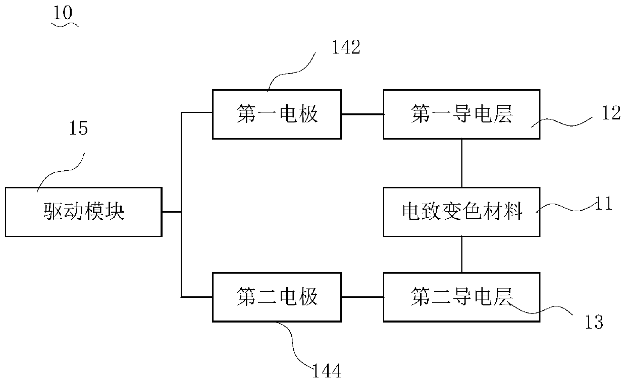
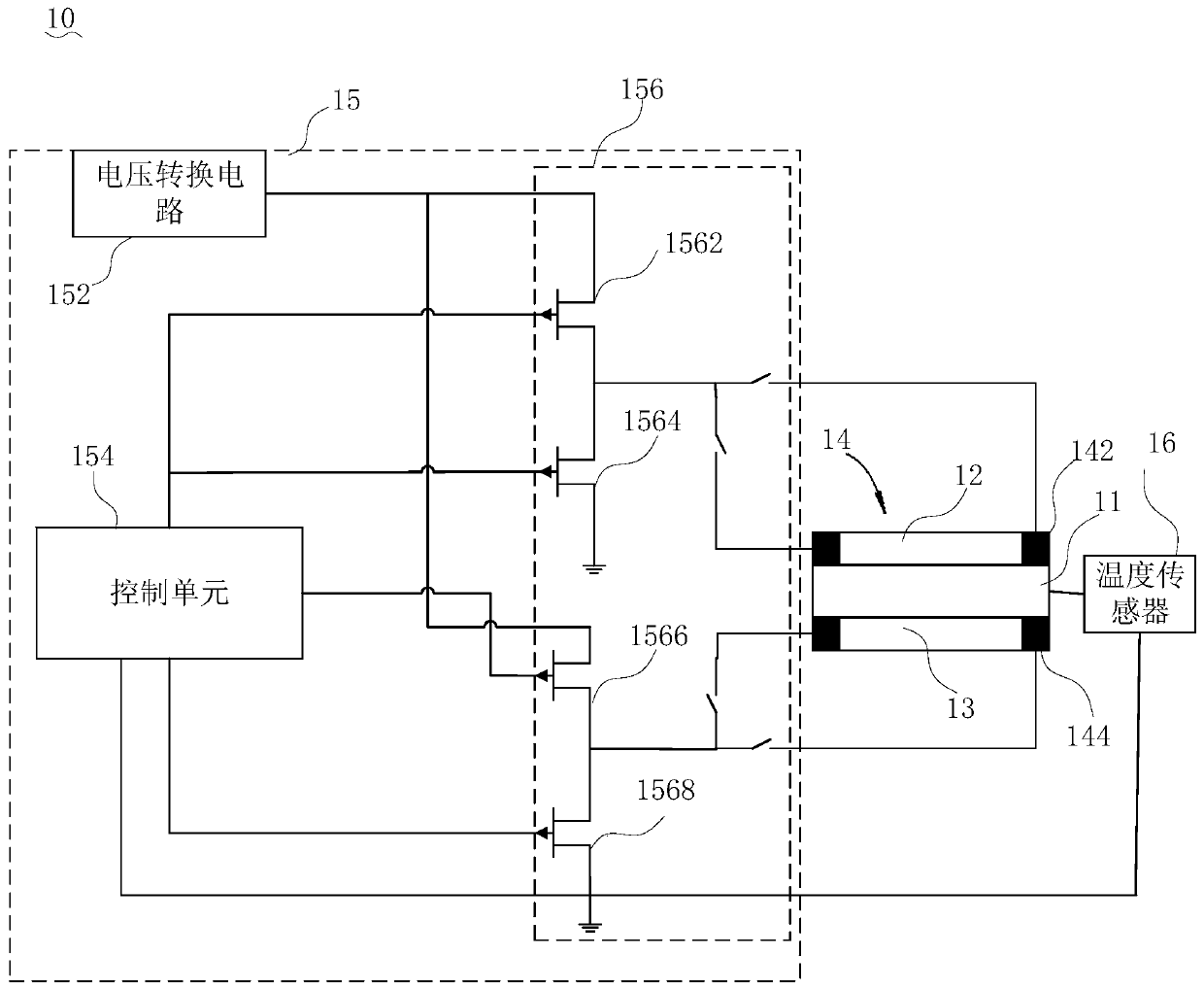
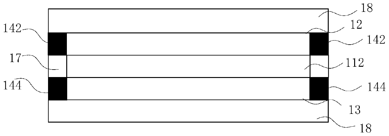
[0025] see figure 1 with figure 2 , The electrochromic device 10 according to the embodiment of the present invention includes an electrochromic material 11 , a first conductive layer 12 , a second conductive layer 13 and a driving module 15 . The first conductive layer 12 and the second conductive layer 13 are respectively disposed on two sides of the electrochromic material 11 . The first conductive layer 12 is provided with a plurality of first electrodes 142 at intervals along the circumferential direction. The second ...


PUM


Abstract

The invention discloses an electrochromic device and an electronic device. The electrochromic device comprises an electrochromic material, a first conductive layer, a second conductive layer, and a drive module. The first conductive layer and the second conductive layer are respectively disposed at the two sides of the electrochromic material. A plurality of first electrodes are arranged along thecircumferential direction of the first conductive layer at intervals; and a plurality of second electrodes are arranged in the circumferential direction of the second conductive layer at intervals. The drive module is used for applying first voltages on the first electrodes and the second electrodes according to a preset sequence to realize coloring of the electrochromic material According to theelectrochromic device in the embodiment of the ivnention, voltages are applied to the plurality of first electrodes and the plurality of second electrodes successively in a time-division manner and thus the position of the connected power supplies of the conductive layers change with the electrode conduction sequence, so that voltage differences of the conductive layers at all positions on the plane change with the electrode conduction sequence. Therefore, electrochromic material ions make horizontal migration stably, so that a phenomenon of a layering reaction caused by long-time electrification of the electrochromic material is avoided.

Description

technical field [0001] The invention relates to the technical field of consumer electronics, and more specifically, to an electrochromic device and electronic equipment. Background technique [0002] In the prior art, electrochromic devices can undergo reversible color changes under the action of an applied electric field. Among them, electrochromic devices can change the color of electrochromic materials by applying voltage to the electrode pairs on both sides of the electrochromic materials. Transmittance, which allows electrochromic materials to switch between a transparent state and a colored state. However, the conductive layer of the electrochromic material has a square resistance, and the voltage difference at each position on the plane is different. A large area of ​​the electrochromic material is charged for a long time, which will cause the electrochromic material ions to migrate laterally. When the electrochromic material achieves fast fading, after the material ...

Claims


Application Information

Patent Timeline
Patent Type & Authority Applications(China)
IPC IPC(8): G02F1/153G02F1/155G02F1/163
CPCG02F1/153G02F1/155G02F1/163
Inventor 李亮
Owner GUANGDONG OPPO MOBILE TELECOMM CORP LTD
Why Eureka
Eureka Blog
Learn More