Array substrate, stretchable display panel and display device

A technology for array substrates and base substrates, which is applied in semiconductor devices, electrical components, circuits, etc., and can solve problems such as the influence of thin film transistor characteristics, affecting display effects, and no shading effect

Active Publication Date: 2019-08-09
BOE TECH GRP CO LTD
View PDF4 Cites 4 Cited by
  • Summary
  • Abstract
  • Description
  • Claims
  • Application Information

AI Technical Summary

Problems solved by technology

[0004] The organic layer or planarization layer (PLN) in the existing display is a transparent material without shading effect. After the distance between the thin film transistor (TFT) and the opening or dividing line is reduced, the exter

Method used


Image

  • Array substrate, stretchable display panel and display device
  • Array substrate, stretchable display panel and display device
  • Array substrate, stretchable display panel and display device

Examples


Embodiment 1

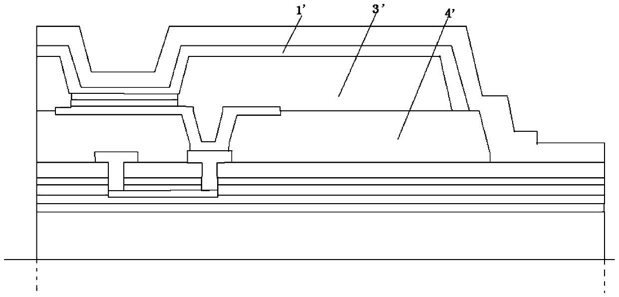
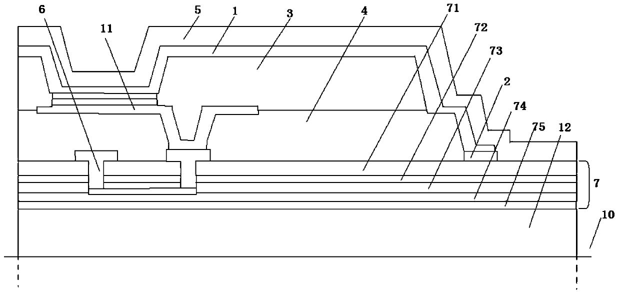
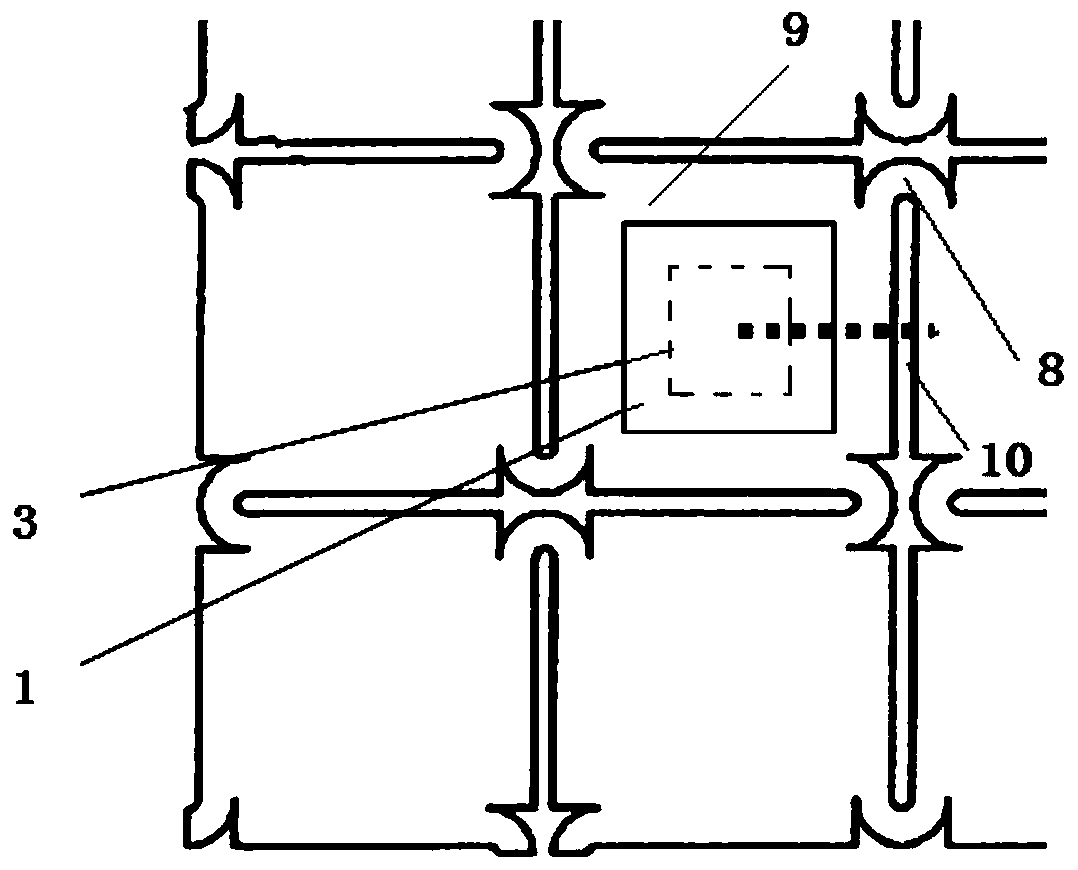
[0038] Reference attached figure 2 , the array substrate provided by the embodiment of the present invention, which includes a base substrate 12, a planarization layer 4, a pixel definition layer 3, a first electrode layer 1, and a thin film encapsulation layer 5, which are sequentially stacked, and the planarization layer 4 and the A thin film transistor 6 is arranged between the base substrates, and a plurality of openings are opened through the thin film encapsulation layer, the first electrode layer 1, the pixel definition layer 3, the planarization layer 4 and the base substrate 12, and a plurality of island 9; specifically, the edge of the first electrode layer 1 extends to cover the sidewall of the planarization layer 4, for shielding the thin film transistor; wherein, the edge of the first electrode layer 1 In contact with the conductor 2 passing through the bridge area 8 between the opening 10 and the island 9 for connecting the adjacent island 9, as a power supply w...

Embodiment 2

[0054] An embodiment of the present invention provides a stretchable display panel, which includes any one of the array substrates in the preceding embodiments:

[0055] The array substrate includes a base substrate 12, a planarization layer 4, a pixel definition layer 3, a first electrode layer 1, and a thin film encapsulation layer 5 that are sequentially stacked, and between the planarization layer 4 and the base substrate 12 A thin film transistor 6 is provided, and a plurality of openings are opened through the thin film encapsulation layer, the first electrode layer 1, the pixel definition layer 3, the planarization layer 4, and the base substrate 12, and a plurality of islands 9 are separated; specifically, The edge of the first electrode layer 1 extends to cover the sidewall of the planarization layer 4 for shielding the thin film transistor; wherein, the edge of the first electrode layer 1 is in contact with the conductor 2, The conductor 2 passes through the bridge r...

Embodiment 3

[0057] A display device provided by an embodiment of the present invention includes the stretchable display panel mentioned in the foregoing embodiments.


PUM


Abstract

The invention discloses an array substrate, a stretchable display panel and a display device, and relates to the technical field of electronic display devices. The array substrate includes a base substrate, a planarization layer, a pixel defining layer, a first electrode layer, and a thin film encapsulation layer which are successively stacked; a thin film transistor is disposed between the planarization layer and the base substrate; a plurality of openings are disposed to pass through the thin film encapsulation layer, the first electrode layer, the pixel defining layer, the planarization layer, and the base substrate to define a plurality of islands spaced apart; the edge of the first electrode layer extends to a sidewall covering the planarization layer for shielding the thin film transistor against light; the edge of the first electrode layer is in contact with a conductor; and the conductor passes through a bridge region arranged between the openings and the islands and used for connecting adjacent islands in order to be used as a power wire for connecting the first electrode layers of the adjacent islands.

Description

technical field [0001] The present invention relates to the technical field of electronic display devices, in particular to an array substrate, a display panel and a display device. Background technique [0002] Stretchable displays need to dig holes or set dividing lines on the display substrate and the film layer above the substrate, so that the display substrates form a plurality of islands distributed in an array and separated from each other, and each of the plurality of islands Islands are connected by a plurality of bridges to make the display substrate stretchable; the openings or dividing lines are used to set the camera or stretch. [0003] There is an invalid area between the opening or dividing line and the thin film transistor (TFT) in the existing stretchable display. At present, electronic screen products tend to increase the display area. In order to increase the display area, the opening or dividing line must be reduced The inactive area between the thin fi...

Claims


Application Information

Patent Timeline
IPC IPC(8): H01L27/12
CPCH01L27/124
Inventor 王品凡
Owner BOE TECH GRP CO LTD
Why Eureka
Try Eureka