Method for reducing organic matter on silicon block surface and method for preparing single crystal silicon

A technology of organic matter and silicon block, which is applied in the direction of surface etching composition, single crystal growth, single crystal growth, etc., can solve problems such as unclear carbon pollution, and achieve the effect of reducing the concentration of organic matter and avoiding wear

Active Publication Date: 2020-10-30
XIAN ESWIN SILICON WAFER TECH CO LTD
View PDF1 Cites 0 Cited by
  • Summary
  • Abstract
  • Description
  • Claims
  • Application Information

AI Technical Summary

Problems solved by technology

[0008] Before the raw silicon block is prepared by the Czochralski method, it needs to go through multiple steps, such as transportation, etching, packaging, unpacking, etc. At present, it is impossible to analyze which step involves the pollution of carbon-containing substances, and it is completely It is not clear why carbon pollution occurs

Method used


Image

  • Method for reducing organic matter on silicon block surface and method for preparing single crystal silicon
  • Method for reducing organic matter on silicon block surface and method for preparing single crystal silicon
  • Method for reducing organic matter on silicon block surface and method for preparing single crystal silicon

Examples


preparation example Construction

[0101] The embodiment of the present invention discloses a method for preparing monocrystalline silicon, which is prepared by the Czochralski method by using the silicon block described in the above technical solution as a raw material.

[0102] The invention also discloses a single crystal silicon, which is produced by the method described in the above technical solution, and the concentration of carbon-containing impurities is below 50ppba.

Embodiment 1

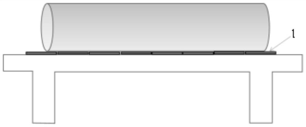
[0105] Breaking the silicon ingot into silicon blocks on a Teflon plate, and then using the Teflon plate to transport the silicon blocks above the etching container;

[0106] Two pillars are arranged between the two opposite side walls of the etching container, and the two pillars divide the etching container into a first area, a second area and a third area; the first area, the second The volume of the area and the third area are equal.

[0107] Four side panels surrounded by a square are arranged in the first area;

[0108] Four side panels surrounded by a square are arranged in the second area;

[0109] Four side panels forming a square are arranged in the third area;

[0110] There is a gap between the side wall and the side panel of the etching container.

[0111] Cooperating with the etching container, the length of one side of the Teflon plate is equal to the distance between the two pillars.

[0112] Tilt the Teflon plate to slide the silicon block into the etching...


PUM

PropertyMeasurementUnit
thicknessaaaaaaaaaa

Abstract

The invention relates to the field of polysilicon, and especially relates to a method for reducing organic matters on the surface of silicon blocks, and a preparation method of monocrystalline silicon. The method for reducing organic matters on the surface of the silicon block comprises the following steps: breaking a silicon ingot into a Teflon plate to form the silicon blocks, and then transporting the silicon blocks to a position over an etching container by using the Teflon plate; tilting the Teflon plate to make the silicon blocks slide into the etching container; etching the silicon blocks in the etching container, and discharging an etching liquid after the etching treatment; ad sleeving the opening of the etching container with a packaging bag, turning over the etching container tomake the etched silicon blocks directly fall into the packaging bag in order to complete the packaging. The reduction method completely realizes the gloveless operation and avoids the abrasion generated during transportation of the silicon blocks by a manipulator and the like. An experimental result shows that the reduction method of the present invention can effectively reduce the concentrationof the organic matters on the surface of the raw material silicon blocks.

Description

technical field [0001] The invention relates to the field of polycrystalline silicon, in particular to a method for reducing organic matter on the surface of a silicon block and a method for preparing single crystal silicon. Background technique [0002] Cs refers to a substance formed by replacing a part of silicon atoms in silicon crystals with carbon atoms, which belongs to carbon-containing impurities inside silicon crystals. In order to improve the quality of monocrystalline silicon, it is necessary to reduce the carbon-containing impurities in monocrystalline silicon products as much as possible. Monocrystalline silicon can be produced by the Czochralski method, in which polycrystalline silicon blocks are used as raw materials. [0003] For the Cs concentration in the silicon block as the raw material of the Czochralski process, the following improvements have been made in the preparation method: [0004] Reducing the use of carbon materials when manufacturing polysi...

Claims


Application Information

Patent Timeline
Patent Type & Authority Patents(China)
IPC IPC(8): C30B35/00C30B15/00C30B29/06C09K13/08
CPCC09K13/08C30B15/00C30B29/06C30B35/007
Inventor 宮尾秀一同嘉锡
Owner XIAN ESWIN SILICON WAFER TECH CO LTD
Why Eureka
Try Eureka