Array substrate and manufacturing method thereof, display panel and display module

A technology for array substrates and display panels, applied in the fields of array substrates and their manufacture, display panels and display modules, can solve the problems of reducing the pull-out force test of the single-layer area width and the difficulty of COF pull-out force guarantee, and achieve increased Effect of pulling force and increasing contact area

Active Publication Date: 2022-04-22
BOE TECH GRP CO LTD +1
View PDF0 Cites 0 Cited by
  • Summary
  • Abstract
  • Description
  • Claims
  • Application Information

AI Technical Summary

Problems solved by technology

[0003] However, in order to achieve ultra-narrow bezels, it is necessary to reduce the width of the single-layer region of COF, which in turn makes it difficult to guarantee the pull-out force of COF, resulting in the irreconcilability of reducing the width of the single-layer region and passing the pull-out force test of COF contradiction

Method used


Image

  • Array substrate and manufacturing method thereof, display panel and display module
  • Array substrate and manufacturing method thereof, display panel and display module
  • Array substrate and manufacturing method thereof, display panel and display module

Examples


no. 1 example

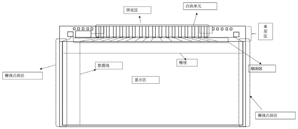
[0038] see figure 1 The array substrate provided by the first embodiment of the present invention includes a display area, a fan-out area (Fan-out) located on one side of the display area, a single-layer area located outside the fan-out area, and a single-layer area located between the display area and the single-layer area. side gate line bump area. The single-layer area is further divided into binding areas. Wherein, the data line and the gate line are set in the display area; the bump unit is set in the binding area for binding with the circuit board. The circuit board is, for example, a Chip On Film (COF for short). A grid line bump is arranged in the grid line bump area, which is connected to the grid line and connected to the bump unit through the silver paste in the single layer area.

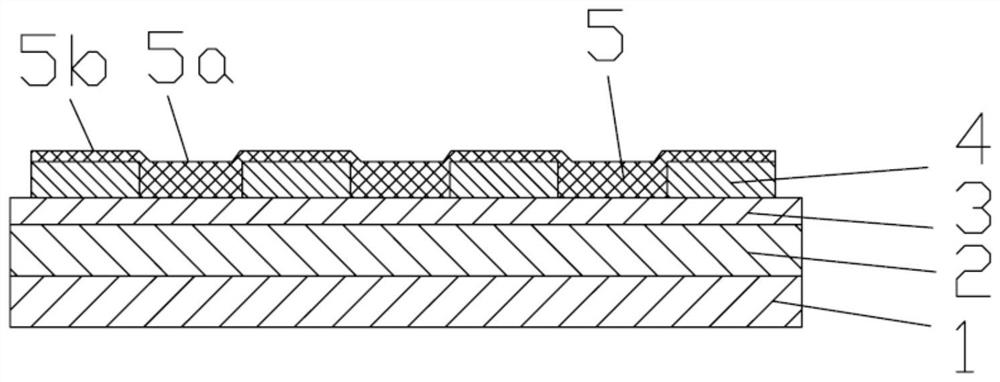
[0039] see figure 2 , the array substrate includes a glass substrate 1, a buffer layer 2 and a planar layer 3 sequentially arranged on the glass substrate 1, and the bump unit inclu...

no. 2 example

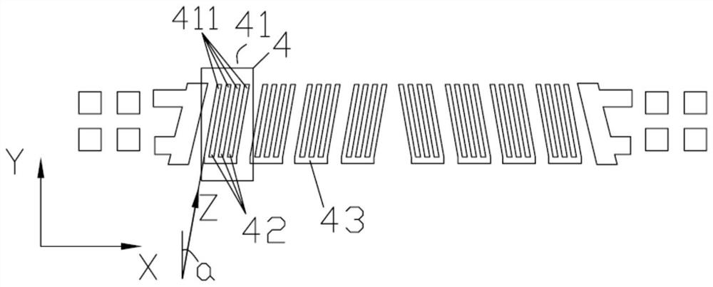
[0045] exist image 3 , in the Z direction, there is only one block 411, but the present invention is not limited thereto, such as Figure 4 As shown, the array substrate provided by the second embodiment of the present invention, compared with the above-mentioned first embodiment, also includes a bump unit, and only the differences between this embodiment and the above-mentioned first embodiment will be described in detail below.

[0046] Specifically, the bump unit includes a plurality of grid line bump layers 4' arranged at intervals along the X direction, and each grid line bump layer 4' includes a main body part 41' and a plurality of hollows arranged in the main body part 41'. Section 42'. The main body 41' includes a plurality of sub-blocks 411' arranged at intervals along the X direction and the Z direction, that is, the plurality of sub-blocks 411' are arranged in an array in the X direction and the Z direction, and two adjacent sub-blocks 411 'The space between con...

no. 3 example

[0049] Such as Figure 5 As shown, the array substrate provided by the third embodiment of the present invention, compared with the above-mentioned first and second embodiments, also includes bump units. The following only discusses the difference between this embodiment and the above-mentioned first and second embodiments. The differences are described in detail.

[0050] Specifically, the bump unit includes a plurality of grid line bump layers 4 ″ arranged at intervals along the X direction, and each grid line bump layer 4 ″ includes a main body 41 ″ and a plurality of hollows arranged in the main body 41 ″ Part 42". The main body part 41" includes a plurality of blocks 411" arranged at intervals along the Z direction, and the space between two adjacent blocks 411" forms a hollow part 42". Thus, in the Z direction, the gate The line bump layer 4" has a concave-convex structure, so that the surface of the data line bump layer 5 covering it and away from the gate line bump la...


PUM


Abstract

The present invention provides an array substrate and its manufacturing method, a display panel and a display module. The array substrate includes data lines and gate lines arranged in the display area, and a bump unit arranged in the binding area. The bump unit includes: A plurality of gate line bump layers arranged on the same layer as the gate lines, each gate line bump layer is connected to each data line in one-to-one correspondence, each gate line bump layer includes a main body and a plurality of gate line bump layers arranged in the main body a hollow part; and a data line bump layer set on the same layer as the data line, the data line bump layer covers all the gate line bump layers, and the sum of the thickness of the data line bump layer and each main body is less than the data line bump layer The thickness of the block layer at each cutout location. The array substrate provided by the present invention ensures that the COF pull-out force meets the requirements under the same condition as the width of the single-layer region adopted in the prior art, thereby realizing the preparation of ultra-narrow frame products.

Description

technical field [0001] The invention relates to the field of display technology, in particular to an array substrate and a manufacturing method thereof, a display panel and a display module. Background technique [0002] With the advent of the "full screen" era, high screen-to-body ratio display screens are favored by consumers. In order to adapt to this trend, screen manufacturers have adopted COF (Chip On Film, often called chip-on-film) module technology. That is, the driver IC is fixed on the flexible circuit board to reduce the space occupied by the frame of the screen and realize the preparation of ultra-narrow frame products. [0003] However, in order to achieve ultra-narrow bezels, it is necessary to reduce the width of the single-layer region of COF, which in turn makes it difficult to guarantee the pull-out force of COF, resulting in the irreconcilability of reducing the width of the single-layer region and passing the pull-out force test of COF contradiction. F...

Claims


Application Information

Patent Timeline
Patent Type & Authority Patents(China)
IPC IPC(8): G02F1/1362
CPCG02F1/136286G02F1/136227H01L27/124H10K59/131H01L24/13H01L24/14H01L27/1259H01L2224/13012H01L2224/13562H01L2224/14155G02F1/136
Inventor 韩帅徐敬义赵欣唐乌力吉白尔任艳伟于亚楠王跃林智国磊
Owner BOE TECH GRP CO LTD
Why Eureka
Try Eureka