Generation and control method of partial erasing voltage of liquid crystal writing film

A technology of erasing voltage and control methods, which is applied in electrical digital data processing, instruments, calculations, etc., can solve the problems of single voltage, loss of conductive layer, and inability to apply voltages to different conductive areas separately, so as to compensate for output voltage instability , improve business value, improve work efficiency and the effect of user experience

Active Publication Date: 2021-07-30
SHANDONG LANBEISITE EDUCATIONAL EQUIP GRP +1
View PDF6 Cites 0 Cited by
  • Summary
  • Abstract
  • Description
  • Claims
  • Application Information

AI Technical Summary

Problems solved by technology

[0003] Existing products using liquid crystal writing film can only erase all handwriting in the entire liquid crystal writing board by means of energization when erasing handwriting. The erasing method cannot meet the needs, especially when modifying the wrong part of the writing, the existing overall erasing method will cause the loss of the rest of the information that does not need to be modified. How to use the power-on method to realize partial erasing has become an urgent need for users to solve question
[0004] The writing film voltage control method disclosed in the prior art can only provide a single voltage for the conductive layer, and use the electric field formed between the two conductive layers to realize the overall erasing of the writing area
This voltage control method cannot apply voltages to different conductive areas separately, and cannot form effective voltage control for different partial erasing areas, and cannot achieve the purpose of partial erasing

Method used


Image

  • Generation and control method of partial erasing voltage of liquid crystal writing film
  • Generation and control method of partial erasing voltage of liquid crystal writing film
  • Generation and control method of partial erasing voltage of liquid crystal writing film

Examples


Embodiment 1

[0087] The embodiment of the present invention discloses a method for generating and controlling local erasing voltage of a liquid crystal writing film, wherein the liquid crystal writing film is located between two conductive layers, and the two conductive layers are respectively divided into two or more than two conductive regions ;

[0088] A voltage is applied to the conductive area of ​​the first conductive layer covering the partially erased area; B voltage is applied to the conductive area of ​​the second conductive layer covering the partially erased area; the A voltage and the B voltage are formed at the spatial overlapping position of the two conductive areas Erase the electric field to achieve local erasure.

[0089] Apply the C voltage to the set conductive areas outside the respective conductive areas of the two conductive layers covering the partially erased area, wherein the set conductive areas can be the respective conductive areas of the two conductive layers...

Embodiment approach

[0100] As a preferred implementation, we set:

[0101] |Vh|=|Va|*2.

[0102] It should be noted that the applied voltages on the two conductive layers are exchanged every set time, so that the electric field formed on the entire liquid crystal writing film has the same magnitude but opposite direction, which can avoid the long-term damage to the liquid crystal writing film. The liquid crystal polarization phenomenon occurs due to the application of an electric field in the same direction. Hereinafter, we refer to the two time periods with different electric field directions as the first half and the second half, respectively.

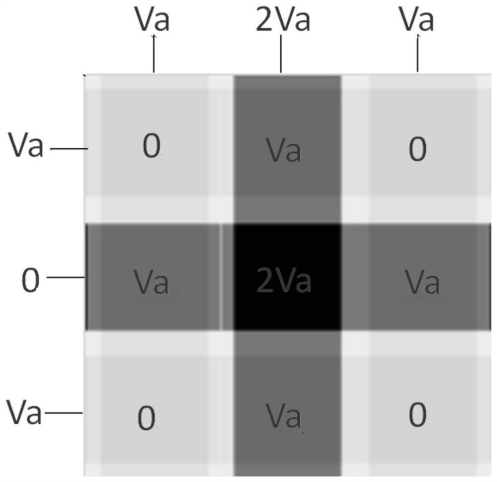
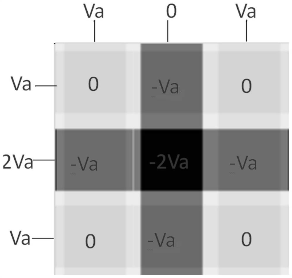
[0103] The voltage applied to each conductive area of ​​the writing film is as follows figure 1 or figure 2 shown. in, figure 1 is the voltage applied in the first half field of each conductive area of ​​the writing film, figure 2 The voltage applied for the second half of each conductive area of ​​the writing film; the order of supply voltages ...

Embodiment 2

[0108] The embodiment of the present invention discloses another method for generating and controlling the partial erasing voltage of the liquid crystal writing film, which overcomes the shortcomings of the control method in the second embodiment, and specifically includes:

[0109] The liquid crystal writing film is located between two conductive layers, and the two conductive layers are respectively divided into two or more conductive regions;

[0110]A voltage is applied to the conductive area of ​​the first conductive layer covering the partially erased area; B voltage is applied to the conductive area of ​​the second conductive layer covering the partially erased area; the A voltage and the B voltage are formed at the spatial overlapping position of the two conductive areas Erase the electric field to achieve local erasure.

[0111] Apply a D voltage to a conductive area set outside the conductive area on the first conductive layer covering the partial erasing area, and a...


PUM


Abstract

The invention discloses a method for generating and controlling local erasing voltage of a liquid crystal writing film. The liquid crystal writing film is located between two conductive layers, and the first conductive layer and the second conductive layer are respectively divided into two or more conductive layers. region, applying A voltage to the conductive region of the first conductive layer covering the partially erased area; applying B voltage to the conductive region of the second conductive layer covering the partially erased area; or, the first conductive layer is divided into two or For more than two conductive areas, the second conductive layer is not divided, and the A voltage is applied to the conductive area of ​​the first conductive layer covering the partial erasing area; the B voltage is applied to the second conductive layer; the present invention can realize local Area erasing, while other areas are not affected by erasing, overcomes the shortcomings of traditional technologies that can only achieve full erasing, improves the user's work efficiency and experience, and improves the commercial value of liquid crystal writing film and its application equipment.

Description

technical field [0001] The invention relates to the technical field of liquid crystal film structures, in particular to a method for generating and controlling a partial erasing voltage of a liquid crystal writing film. Background technique [0002] The working principle of the liquid crystal writing film currently on the market is to use the bistable characteristics of liquid crystals to display and / or erase the written content on the liquid crystal writing board. For example, using cholesteric liquid crystal as a writing film, the writing pressure track of the writing pen is recorded by the pressure acting on the liquid crystal writing board, and then the corresponding writing content is displayed; the structure of the cholesteric liquid crystal is changed by applying an electric field, so that the liquid crystal The writing pressure track on the tablet disappears to enable erasing. [0003] Existing products using liquid crystal writing film can only erase all handwritin...

Claims


Application Information

Patent Timeline
Patent Type & Authority Patents(China)
IPC IPC(8): G06F3/041
CPCG06F3/0412G06F3/0414G06F3/0416
Inventor 李清波史新立
Owner SHANDONG LANBEISITE EDUCATIONAL EQUIP GRP
Why Eureka
Try Eureka