Low-power time-to-digital converter

A time-to-digital converter technology, which is used in time-to-digital converters, electrical unknown time interval measurement, devices for measuring time intervals, etc. Effect

Active Publication Date: 2019-08-27
FUDAN UNIV
2 Cites 4 Cited by

AI-Extracted Technical Summary

Problems solved by technology

However, the results obtained by the charging and discharging of resistors and capacitors are not completely linear. Therefore, the input range of the ...

Method used

[0045] To sum up, the low-power time-to-digital converter of the present invention improves the precision and sensitivity of the time-to-digital converter by amplifying the phase difference, and controls the switches S1-S3 to turn off different time periods. The circuit that nee...

Abstract

The invention relates to a low-power time-to-digital converter. The low-power time-to-digital converter comprises a pre-amplifier and a successive approximation register type analog-digital converter;signals in a pseudo-differential form are input to the pre-amplifier; through a phase frequency detector of the pre-amplifier, a phase inverter, a passive amplifier composed of an N-type MOS capacitor, and a source follower, the input time-domain signals are converted into voltage signals, and the voltage signals are amplified; and finally, the voltage signals are input to the successive approximation register type analog-to-digital converter to be converted into digital signals. The passive amplifier composed of the N-type MOS capacitor is used, so that the precision of the time-to-digital converter can be improved. The phase inverter is turned off after the input signals are sampled, and the source follower is turned off in a restoration state; and two mechanisms can be used for avoiding unnecessary power consumption for the low-power time-to-digital converter so as to achieve the purpose of low power consumption.

Application Domain

Time-to-digital converters

Technology Topic

Image

  • Low-power time-to-digital converter
  • Low-power time-to-digital converter
  • Low-power time-to-digital converter

Examples

  • Experimental program(1)

Example Embodiment

[0033] Hereinafter, the present invention will be more fully described in reference embodiments in conjunction with the drawings. The present invention provides preferred embodiments, but should not be considered as limited to the embodiments set forth herein.
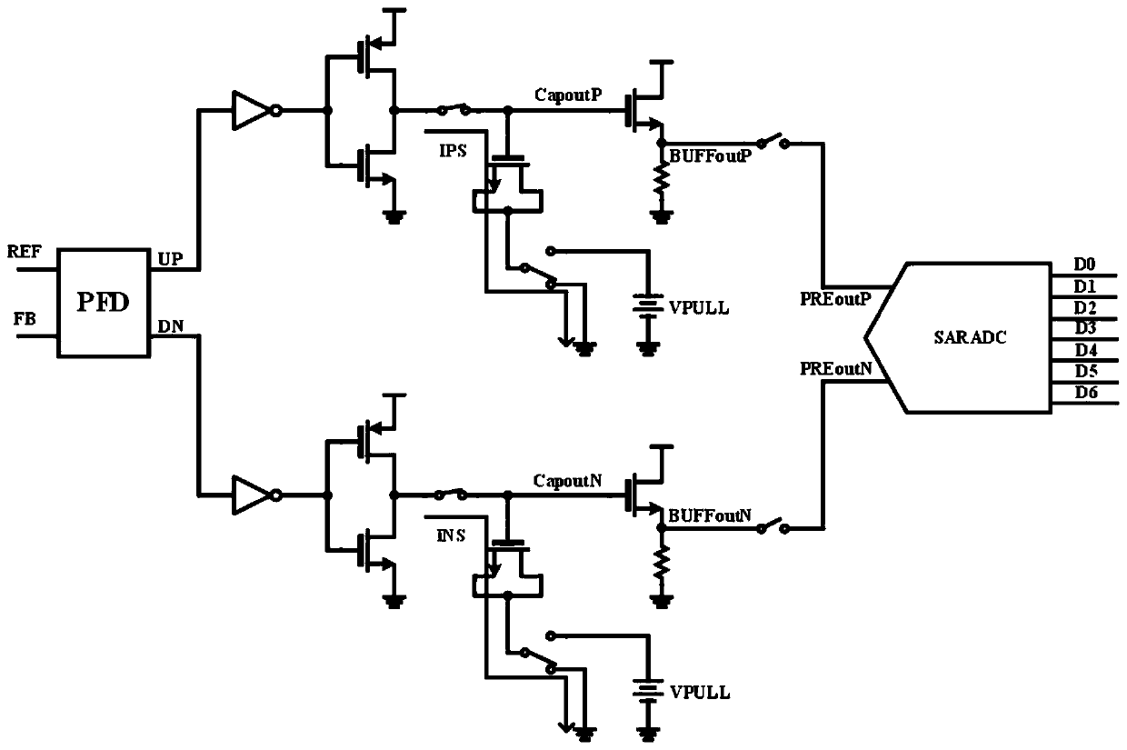
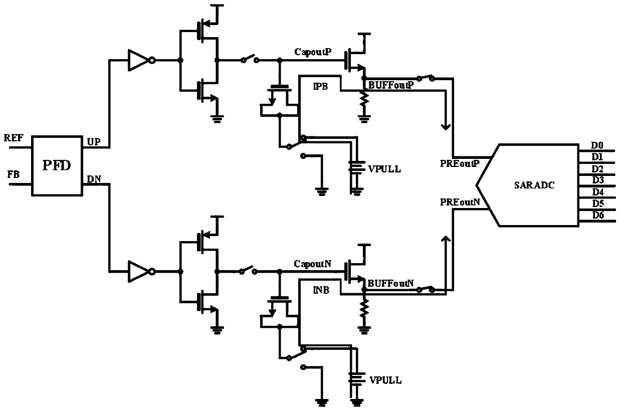
[0034] The present invention provides a low-power time-to-digital converter, which is figure 1 The circuit architecture shown includes a pre-amp (Pre-amp) and a successive approximation register analog-to-digital converter (SARADC); the input signal is input into the pre-amplifier in the form of pseudo-differential for amplification, and then by successive approximation The register type analog-to-digital converter converts into a digital signal. Among them, the design principle of the pre-amplifier is to obtain the phase difference between the two input clock signals, and the phase difference is input into the inverter in the form of a pulse and converted into a voltage before amplifying. The analog-to-digital converter of the successive approximation register type can use a common architecture, which is not limited in the present invention.
[0035] In the pre-amplifier of the present invention, the phase frequency detector PFD (Phase Discriminator/Frequency Discriminator) obtains two output phase difference signals, using an inverter, a passive amplifier (NCB-PA) composed of an N-type MOS capacitor, and a source The pole followers are respectively converted into voltage signals and amplified, and finally input to the successive approximation register type analog-to-digital converter to convert into digital signals
[0036] Specifically, the phase frequency detector receives the input reference clock signal REF and the input signal FB. The phase frequency detector output signals UP and DN are divided into two channels, which are processed by corresponding devices and then connected to the successive approximation register analog digital Each converter includes an inverter I1, an inverter I2, a passive amplifier NCB-PA·I3 composed of N-type MOS capacitors, a source follower I4, and switches S1, S2, and S3.
[0037] Among them, the inverter I2 includes a P-type MOS tube M0 and an N-type MOS tube M1. The gates of M0 and M1 are connected as the input terminal and connected to the output terminal of the inverter I1; the source of M0 is connected to the power supply, the source of M1 is grounded; the drains of M0 and M1 are connected as the output terminal, and the NCB is connected through the switch S1 -PA and source follower I4.
[0038] The gate of the N-type MOS transistor in the NCB-PA is connected to the source follower I4 and the switch S1, the source and drain are connected to the switch S2, and the switch S2 is switched to connect the DC voltage VPULL or ground.
[0039] The N-type MOS tube in the source follower I4 has its gate connected to switches S1 and NCB-PA, and its drain connected to the power supply; the source is grounded through a resistor, and is also used as an output terminal connected to the switch S3 to successively approach the register type The corresponding port of the analog-to-digital converter.
[0040] In the figure, CapoutP and CapoutN are the output signals of the two NCB-PAs, BUFFoutP and BUFFoutN are the output signals of the two source followers, PREoutP and PREoutN are the two output signals of the pre-amplifier, D0-D6 are the successive approximation register type The output signal of the analog-to-digital converter.
[0041] The specific operation of the low-power time-to-digital converter of the present invention is divided into three states, and its circuit will sequentially enter the sampling state, the amplification state, and the restoration state according to the control of the clock. Such as figure 2 As shown, when the circuit is in the sampling state, the phase frequency detector will detect the phase difference between the two clock signals REF and FB to obtain the two output signals UP and DN. Switch S1 is closed, switch S2 is grounded, and switch S3 is opened. The output of the inverter charges the NCB-PA for sampling; IPS and INS correspond to two NCB-PAs, which are the charging directions when the pre-amplifier is working in the sampling state: ground through switches S1, NCB-PA, and switch S2; sampling After completion, the circuit enters the amplification state.
[0042] Such as image 3 As shown, when the circuit is in the amplified state, switch S1 is opened, switch S2 is connected to DC voltage VPULL, and switch S3 is closed. At this time, NCB-PA is connected to DC voltage VPULL, so that two NCB-PAs get an amplified output respectively The voltages CapoutP and CapoutN, and then the output voltages CapoutP and CapoutN pass through their respective source followers to charge the capacitor array in the successive approximation register-type analog-to-digital converter and convert them to obtain a digital output signal. IPB and INB are the charging directions when the pre-amplifier is working in the amplified state: through the DC voltage VPULL, the switch S2, the NCB-PA, the gate to the source of the source follower, and the successive approximation of the register type analog-to-digital converter. Finally, the circuit enters the restoration state.
[0043] Such as Figure 4 As shown, when the circuit is in the restoring state, switch S1 is closed, switch S2 is grounded, and switch S3 is open. At this time, the N-type MOS tube M1 in inverter I2 is working in the conducting state, so the charge in NCB-PA will be affected by M1 turns on and flows to the ground. IPH and INH are the discharge directions when the pre-amplifier is working in the restoring state: through the drain to the source of M1 in the NCB-PA, switch S1, and inverter I2. The purpose of the restoration state is to clear the charge in the NCB-PA to avoid the accumulation of charges in the NCB-PA causing the output of the entire circuit to diverge when the system enters the next sampling and amplification state.
[0044] In order to improve the accuracy of the time-to-digital converter, the present invention uses a method of amplifying the phase difference to improve the sensitivity of the time-to-digital converter. For example, the preamplifier gain in the present invention is about 13mV/1ps, that is, the minimum phase difference that can be detected by the preamplifier in the present invention is 1ps, and this 1ps phase difference can be converted into a 13mV voltage signal. The operating principle of phase difference amplification is to connect the NCB-PA after the inverter, which is composed of N-type MOS capacitors. When the low-power time-to-digital converter is working in the sampling state, the N-type MOS capacitor in NCB-PA works in the strong inversion area, and the N-type MOS capacitor will produce a larger capacitance value. When working in amplifying state, the N-type MOS capacitor in NCB-PA works in the depletion area, and the N-type MOS capacitor value will attenuate. Therefore, according to the principle of charge conservation, the gain of NCB-PA is approximately the same as that of the N-type MOS capacitor working in strong reverse The ratio of the area to the depletion area.
[0045] In summary, the low-power time-to-digital converter of the present invention improves the accuracy and sensitivity of the time-to-digital converter by amplifying the phase difference, and is controlled by switches S1-S3 to turn off unused ones at different periods of time. Circuit, avoid the overall circuit to generate additional power consumption, in order to achieve the design goal of low power consumption. The invention can be applied to the design of digital phase-locked loop to reduce the quantization error of the digital phase-locked loop.
[0046] The embodiments of the present invention are described above through specific specific examples, and those skilled in the art can easily understand other advantages and effects of the present invention from the content disclosed in this specification. The present invention can also be implemented or applied through other different specific embodiments, and various details in this specification can also be modified or changed based on different viewpoints and applications without departing from the spirit of the present invention.
[0047] Although the content of the present invention has been described in detail through the above preferred embodiments, it should be recognized that the above description should not be considered as limiting the present invention. After those skilled in the art have read the above content, various modifications and substitutions to the present invention will be obvious. Therefore, the protection scope of the present invention should be defined by the appended claims.

PUM

no PUM

Description & Claims & Application Information

We can also present the details of the Description, Claims and Application information to help users get a comprehensive understanding of the technical details of the patent, such as background art, summary of invention, brief description of drawings, description of embodiments, and other original content. On the other hand, users can also determine the specific scope of protection of the technology through the list of claims; as well as understand the changes in the life cycle of the technology with the presentation of the patent timeline. Login to view more.

Similar technology patents

Method and device for forecasting reservoir yield

InactiveCN101906966AHigh precisionSurveyWellheadVolume factor
Owner:PETROCHINA CO LTD

Classification and recommendation of technical efficacy words

  • High precision
  • Reduce quantization error

Semantic enhanced hash medical image retrieval method based on mixed attention

PendingCN113889228AReduce quantization errorHigh precisionStill image data queryingMedical imagesMachine learningSemantic enhancement
Owner:WUHAN UNIV OF TECH

Dictionary learning static image lossy compression method based on minimum quantization error criterion

ActiveCN107170020AReduce coding costsReduce quantization errorCode conversionImage codingDictionary learningSparse coefficient
Owner:NORTHWESTERN POLYTECHNICAL UNIV

Neural network optimization method and related equipment

PendingCN111950700AReduce quantization errorEfficient in training and useGeometric image transformationCharacter and pattern recognitionEngineeringAlgorithm
Owner:HUAWEI TECH CO LTD
Why Eureka
Try Eureka