OLED display panel and preparation method thereof

A display panel and organic layer technology, applied in electrical components, electrical solid devices, circuits, etc., can solve the problems that the display area is vulnerable to water and oxygen erosion and affect product reliability, and achieve the effect of improving reliability

Active Publication Date: 2019-09-10
WUHAN CHINA STAR OPTOELECTRONICS SEMICON DISPLAY TECH CO LTD
View PDF4 Cites 19 Cited by
  • Summary
  • Abstract
  • Description
  • Claims
  • Application Information

AI Technical Summary

Problems solved by technology

[0003] The present invention provides an OLED display panel and a preparation method thereof to solve the problem that in the existing OLED display panel, due to the adoption of a through-hole de

Method used


Image

  • OLED display panel and preparation method thereof
  • OLED display panel and preparation method thereof
  • OLED display panel and preparation method thereof

Examples


preparation example Construction

[0042] Such as Figure 4 As shown, the present invention also provides a method for preparing an OLED display panel, comprising the following steps:

[0043] S10, providing a substrate, defining a wall area on the substrate;

[0044] S20, preparing several layers of inorganic layers, at least one first metal block, and several layers of organic layers on the substrate, wherein the first metal block is located in the barrier area;

[0045] S30, forming a via hole in the retaining wall region, the via hole passing through several layers of the inorganic layer and several layers of the organic layer, and the via hole exposes a side surface of the first metal block;

[0046] S40, using an etchant to etch the first metal block to form a groove on the sidewall of the via hole;

[0047] S50, forming a light emitting layer on the organic layer, wherein the light emitting layer is discontinuous at the groove of the via hole;

[0048] S60, forming an encapsulation layer on the organi...

Embodiment 1

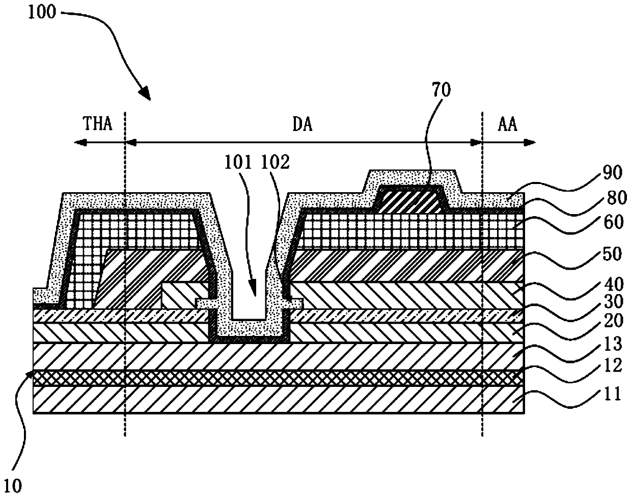
[0053] Such as image 3 As shown, this embodiment provides an OLED display panel 100, including a substrate 10, several inorganic layers disposed on the substrate, a light emitting layer 80 disposed on the organic layer, and a light emitting layer disposed on the light emitting layer. 80 on the packaging layer, and the via 101.

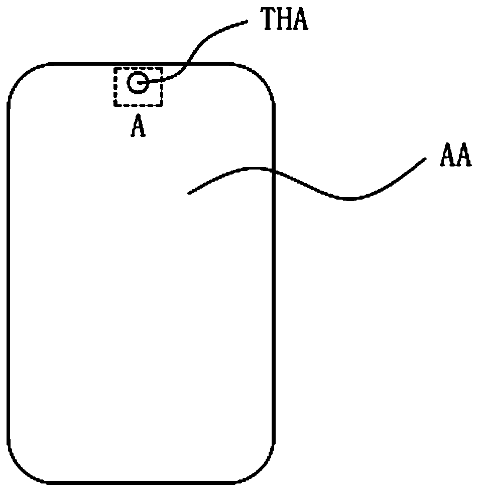
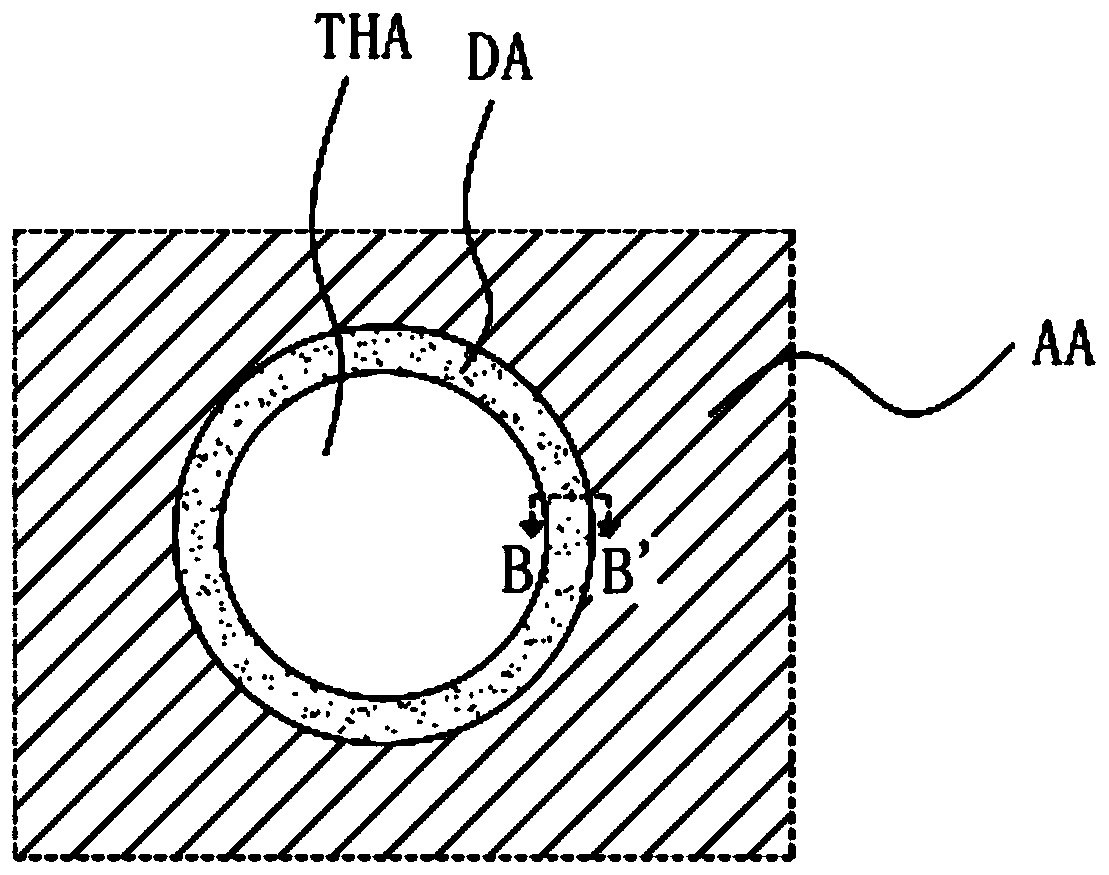
[0054] The OLED display panel 100 defines a display area AA, a through hole area THA, and a wall area DA disposed between the display area AA and the through hole area THA.

[0055] The display area AA is used to realize color display, the through hole area THA is used to place a camera, and the wall area DA is used to disconnect the light emitting layer 80 so that the light emitting layer 80 is on the substrate 10 is discontinuous, so as to prevent water and oxygen from corroding the part of the light emitting layer 80 located in the display area.

[0056] The via hole 101 is disposed in the retaining wall area DA, the via hole 101 penetrates throu...

Embodiment 2

[0089] The first metal block 102' in this embodiment is prepared on the same layer as the source and drain electrodes, and the position of the groove 102 is different from that in Embodiment 1. The groove 102 in this embodiment is prepared by In the case of the drain metal, the patterned metal block in the wall area DA is retained, and the metal block is etched away to be formed.

[0090] Such as Figure 12 As shown, the two grooves 102 in this embodiment are arranged at intervals between the interlayer insulating layer 40 and the flat layer 50, the depth of the grooves 102 is 730 nanometers, and other structures are the same as those in the embodiment. One is the same, so I won't repeat them here.

[0091] Such as Figure 9As shown, when depositing the source-drain metal film layer on the interlayer insulating layer 40, the two patterned metal blocks (namely the first metal block 102') in the barrier area DA are reserved.

[0092] Such as Figure 10 As shown, after the pi...


PUM

PropertyMeasurementUnit
Thicknessaaaaaaaaaa
Thicknessaaaaaaaaaa

Abstract

Provided is an OLED display panel on which a retaining wall area is defined. The display panel includes a substrate, several inorganic layers, several organic layers, a light emitting layer, a packaging layer and a via hole. The via hole penetrates through the inorganic layers and the organic layers, and is located in the retaining wall area. At least one groove is arranged in the side wall of thevia hole. The light emitting layer is discontinuous at the grooves. By forming a deep via hole between the scribe line edge and the display area edge of a through hole and forming grooves in the sidewall of the via hole, the organic light emitting layer vapor-plated subsequently is disconnected at the grooves, the continuity of the organic light emitting layer at the through hole is blocked, thedisplay area is protected from the erosion of water and oxygen, and the reliability of the product is improved.

Description

technical field [0001] The invention relates to the technical field of display driving, in particular to an OLED display panel and a preparation method thereof. Background technique [0002] Full screen is one of the development directions of OLED (Organic Light-Emitting Diode, Organic Light-Emitting Diode) display technology. The under-screen camera technology can further increase the screen ratio of the screen on the basis of existing technologies, which is conducive to the realization of full-screen design. The current under-screen camera technology mainly has two structures: through hole and blind hole. The through hole design needs to hollow out the substrate in the camera area to form a through hole, which will make the display area vulnerable to water and oxygen erosion, and there is a problem of poor reliability. . Contents of the invention [0003] The present invention provides an OLED display panel and a preparation method thereof to solve the problem that in t...

Claims


Application Information

Patent Timeline
IPC IPC(8): H01L27/32
CPCH10K59/12H10K59/1201
Inventor 余赟
Owner WUHAN CHINA STAR OPTOELECTRONICS SEMICON DISPLAY TECH CO LTD
Why Eureka
Try Eureka