Voltage Trimming Method

A voltage and measurement technology, which is applied in the direction of measuring electricity, measuring electrical variables, electronic circuit testing, etc., can solve the problem of long search time for voltage trimming methods, and achieve the goal of overcoming the range that does not meet the requirements and avoiding long search time Effect

Active Publication Date: 2022-01-28
SHANGHAI HUAHONG GRACE SEMICON MFG CORP
View PDF6 Cites 0 Cited by
  • Summary
  • Abstract
  • Description
  • Claims
  • Application Information

AI Technical Summary

Problems solved by technology

[0004] The purpose of the present invention is to provide a voltage trimming method to solve the problem of long search time in the existing voltage trimming method

Method used


Image

  • Voltage Trimming Method
  • Voltage Trimming Method
  • Voltage Trimming Method

Examples


Embodiment Construction

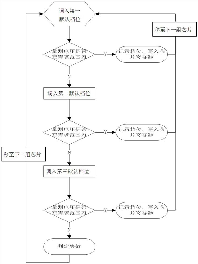
[0030] The voltage trimming method proposed by the present invention will be further described in detail below in conjunction with the accompanying drawings and specific embodiments. Advantages and features of the present invention will be apparent from the following description and claims. It should be noted that all the drawings are in a very simplified form and use imprecise scales, and are only used to facilitate and clearly assist the purpose of illustrating the embodiments of the present invention.

[0031] The core idea of ​​the present invention is to provide a voltage trimming method to solve the problem of long search time in the existing voltage trimming method.

[0032] In order to realize the above idea, the present invention provides a voltage trimming method, the voltage trimming method includes: establishing a program sub-function in the testing machine; placing the wafer on the probe station, and adjusting the first default gear to into the testing machine; t...


PUM


Abstract

The invention provides a voltage trimming method. A program subfunction is established in a testing machine; a wafer is placed on a probe station, and the first default gear is transferred to the testing machine; A group of chips on the wafer are contact-measured to obtain a plurality of first measurement voltages; the testing machine judges whether the first measurement voltages are within the required range, and if so, the program subfunction records The gear corresponding to the first measurement voltage, and write the gear corresponding to the first measurement voltage into the chip register, the program subfunction calculates the gear with the highest frequency of occurrence at this time, and writes the frequency of occurrence The highest gear is transferred into the testing machine as the first default gear, and moved to the next group of chips for contact measurement on the next group of chips.

Description

technical field [0001] The invention relates to the technical field of semiconductors, in particular to a voltage trimming method. Background technique [0002] Wafer testing, referred to as Chip Probing, is the first stop of semiconductor back-end packaging testing. The purpose of Chip Probing is to ensure that each chip can basically meet the characteristics of the device or design specification (Specification), usually including voltage, current, timing and function. verification. The equipment used in Chip Probing includes a tester (IC Tester), a probe card (Probe Card), a probe station (Prober) and an interface (Mechanical Interface) between the tester and the probe card. [0003] The voltage trimming method is one of the basic operations of the Flash test, and it is the most common in the Chip Probing test. Due to the difference in process size and process structure, the voltage trimming items range from 2 to 8 items. figure 1 It is currently the mainstream 3-time f...

Claims


Application Information

Patent Timeline
Patent Type & Authority Patents(China)
IPC IPC(8): G01R31/28
CPCG01R31/2851
Inventor 王善屹索鑫
Owner SHANGHAI HUAHONG GRACE SEMICON MFG CORP
Why Eureka
Try Eureka