TSV-based multi-chip package structure and method for fabricating same

A multi-chip packaging and chip technology, which is used in semiconductor/solid-state device manufacturing, electrical components, electrical solid-state devices, etc., can solve the problem of limited chip size selection, unfavorable development of diversified chip packaging, etc., and achieve the effect of compact packaging structure.

Pending Publication Date: 2019-10-15
SHANGHAI XIANFANG SEMICON CO LTD
View PDF0 Cites 6 Cited by
  • Summary
  • Abstract
  • Description
  • Claims
  • Application Information

AI Technical Summary

Problems solved by technology

[0005] Therefore, the technical problem to be solved by the present invention is to overcome the multi-chip packaging structure in the prior art. Due to the limitation of the size of the interconnection layer, the sum of the sizes of the chips integrated on the TSV adapter board needs to be smaller than that of the TSV adapter board. The size of the chip, which leads to the limitation of the size selection of the chip, is not conducive to the diversified development of chip packaging, thereby providing a TSV-based multi-chip packaging structure and its preparation method

Method used


Image

  • TSV-based multi-chip package structure and method for fabricating same
  • TSV-based multi-chip package structure and method for fabricating same
  • TSV-based multi-chip package structure and method for fabricating same

Examples


Embodiment 1

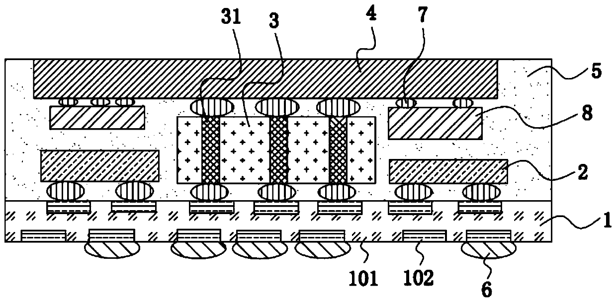
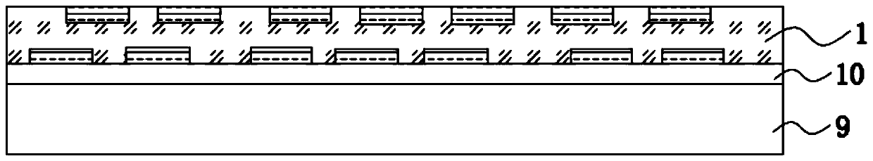
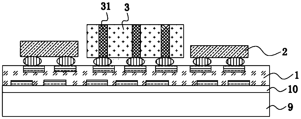
[0038] Such as figure 1 As shown, this embodiment relates to a TSV-based multi-chip packaging structure, including an interconnection structure 1 , a first chip 2 , an interposer 3 , a second chip 4 , a packaging layer 5 and a bump structure 6 .

[0039] Wherein, the first chip 2 and the adapter plate 3 are installed on the interconnection structure 1, and the first chip 2 and the adapter plate 3 are located on the same side of the interconnection structure 1; the second chip 4 is installed on the adapter plate 3 On the top, the second chip 4 is arranged opposite to the interconnection structure 1; the encapsulation layer 5 is arranged on the interconnection structure 1, and the encapsulation layer 5 is used for plastic sealing the first chip 2, the interposer 3 and the second chip 4; bumps The structure 6 is arranged on the interconnection structure 1 and is located on the side opposite to the first chip 2 , and the bump structure 6 is used to realize the electrical connectio...


PUM


Abstract

The present invention relates to the field of chip packaging and in particular to a TSV-based multi-chip package structure and a method for fabricating the same. The multi-chip package structure comprises an interconnection structure; a first chip disposed on the interconnection structure; an adapter plate disposed on the interconnection structure at the same side as well as the first chip, and having a thickness greater than that of the first chip; a second chip disposed on the adapter plate and opposite to the interconnection structure; and a packaging layer. By means of the interconnectionstructure and the adapter plate which has a certain thickness and on which the second chip is mounted, the first chip and the second chip can be located on two planes at different heights, thereby realizing the three-dimensional package of the multiple chips. Compared with the prior art, the package structure provided by the present invention has the size sum of the first chip and the second chipno longer limited by the plan view size of the interconnection structure, thereby expanding the diversified development of the chip packaging structure.

Description

technical field [0001] The invention relates to the field of chip packaging, in particular to a TSV-based multi-chip packaging structure and a preparation method thereof. Background technique [0002] With the development of electronic products in the direction of miniaturization, high performance, and high reliability, the system integration level is also increasing. The 2.5D / 3D integration technology with Through Silicon Via (TSV) as the core has been widely considered to be the future The leading technology in the field of high-density packaging. Compared with traditional 2D packaging, TSV-based 2.5D packaging enables multiple chips to be directly interconnected on the adapter board, which greatly shortens the length of the wiring and reduces signal delay and loss. [0003] The current TSV-based packaging structure usually sets the TSV array directly on a silicon substrate, and at the same time performs wiring on the upper and lower surfaces of the silicon substrate to fo...

Claims


Application Information

Patent Timeline
Patent Type & Authority Applications(China)
IPC IPC(8): H01L23/538H01L23/48H01L23/498H01L21/48H01L21/768
CPCH01L21/4846H01L21/4853H01L21/76898H01L23/481H01L23/49816H01L23/5384H01L23/5386H01L2224/16225H01L2924/15311H01L2924/19105
Inventor 李恒甫曹立强
Owner SHANGHAI XIANFANG SEMICON CO LTD
Why Eureka
Try Eureka