

Array substrate
An array substrate and array technology, applied in nonlinear optics, instruments, optics, etc., can solve problems such as pixel light leakage contrast, and achieve the effect of improving contrast, avoiding light leakage, and reducing intersections or corners
- Summary
- Abstract
- Description
- Claims
- Application Information
AI Technical Summary
Problems solved by technology
Method used
Image

Examples
Embodiment Construction
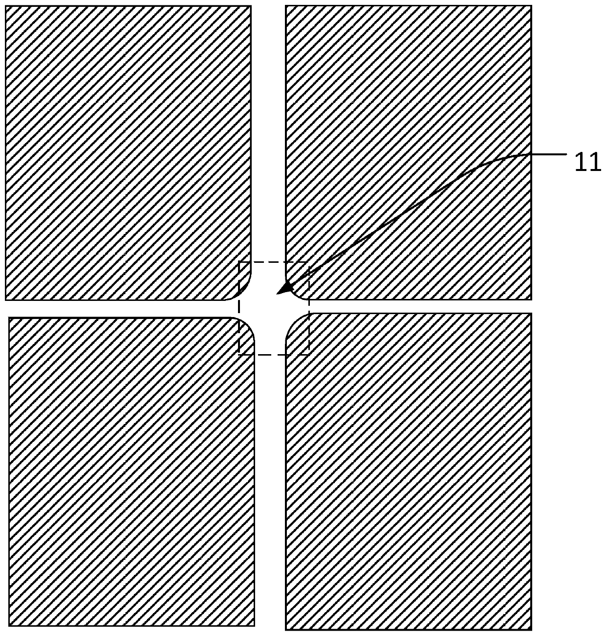
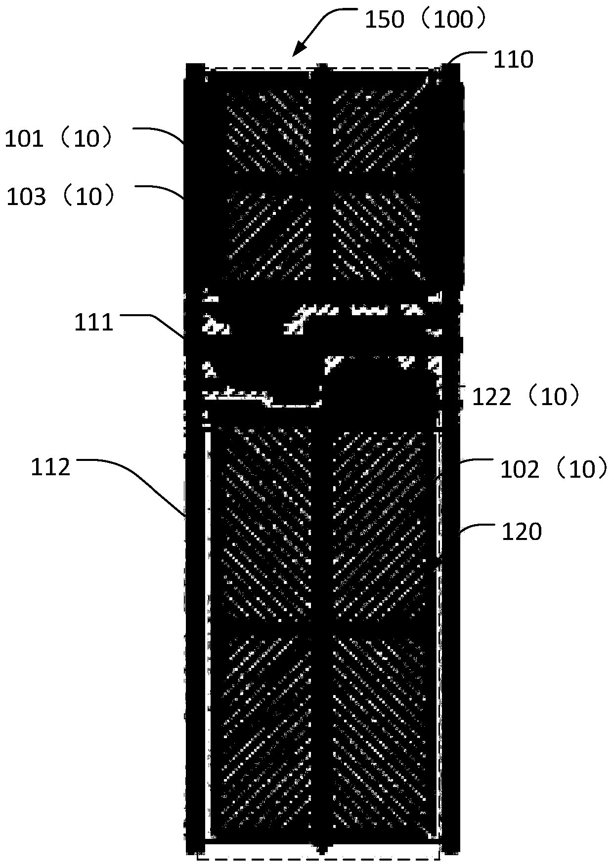
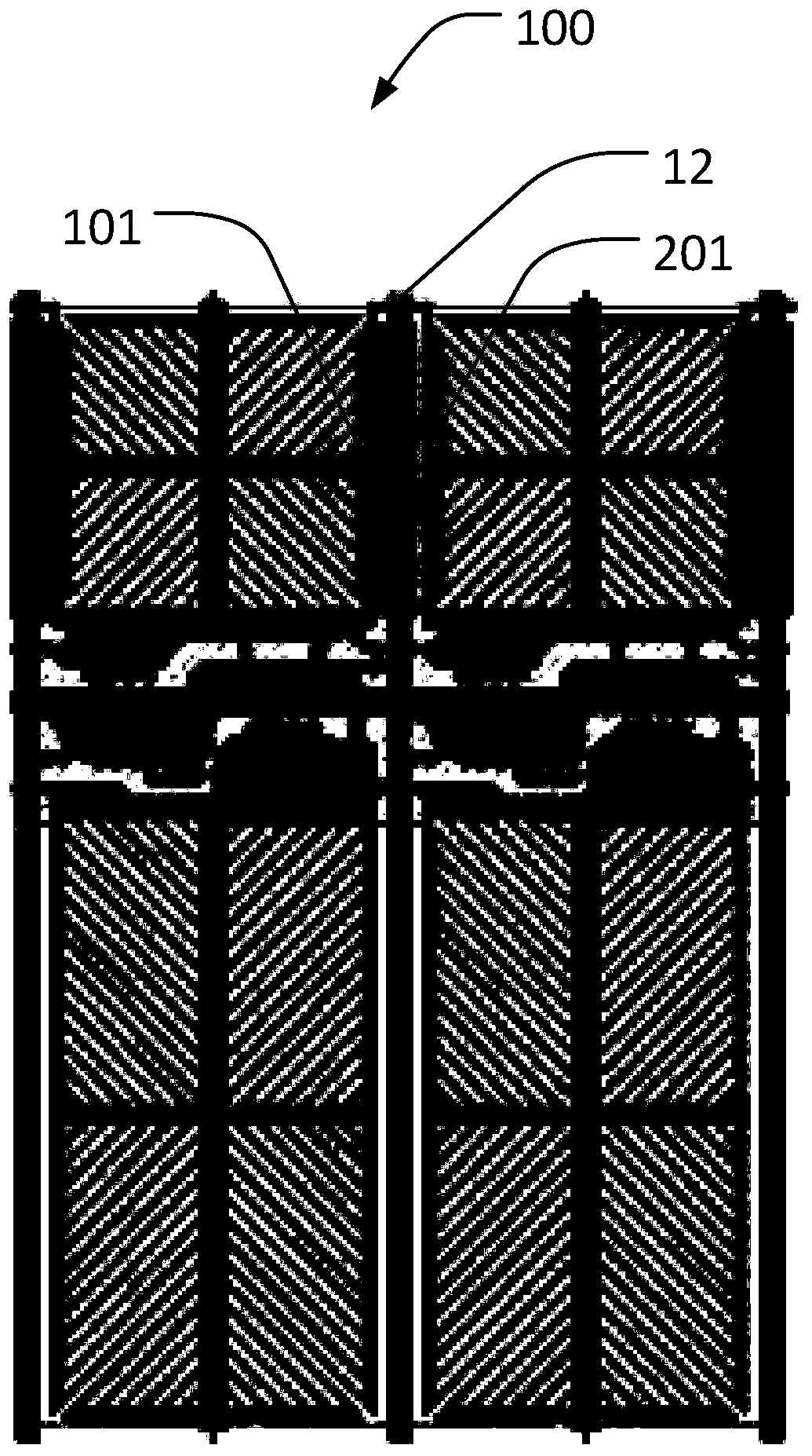
[0033] The following description of various embodiments is made with reference to the accompanying drawings to illustrate specific embodiments in which the invention may be practiced. The directional terms mentioned in the present invention, such as up, down, front, back, left, right, inside, outside, side, etc., are only directions referring to the drawings. The component names mentioned in the present invention, such as first, second, etc., are only used to distinguish different components, which can be better expressed. In the figures, structurally similar elements are denoted by the same reference numerals.
[0034] Embodiments of the present invention will be described in detail herein with reference to the accompanying drawings. This invention may be embodied in many different forms and should not be construed as only the specific embodiments set forth herein. These embodiments are provided to explain the practical application of the invention, so that others skilled i...
PUM
 Abstract
Description
Claims
Application Information