A germanium-silicon-based gallium arsenide material and its preparation method and application
A silicon-based gallium arsenide and gallium arsenide technology, which is applied in semiconductor/solid-state device manufacturing, electrical components, circuits, etc., can solve problems such as poor thermal conductivity, high-density dislocations, and CMOS process incompatibility, and achieve suppression of inversion Domain, the effect of stress release
- Summary
- Abstract
- Description
- Claims
- Application Information
AI Technical Summary
Problems solved by technology
Method used
Image

Examples
Embodiment
[0043] This example is intended to illustrate the germanium-silicon group arsena material of the present invention and the preparation method thereof.
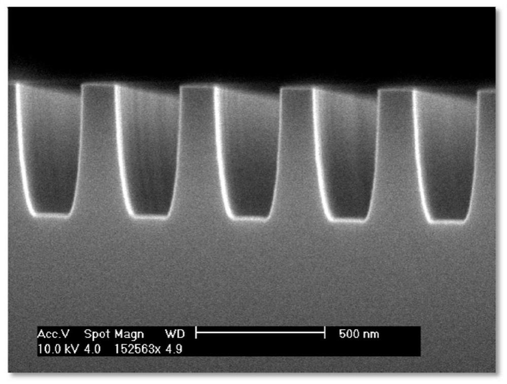
[0044] (1) form a periodic groove structure on silicon substrate:
[0045] The surface of the silicon (100) substrate is used for plasma reinforcing vapor deposition methods, and the growth of SiO 2 Mask; using deep ultraviolet photolithography in SIO 2 The periodic groove structure is constructed in the (110) direction; the surface of the silicon substrate having a periodic groove structure is completed by the reaction ion etching technique; the surface SiO is removed by hydrofluoric acid 2 Mask;
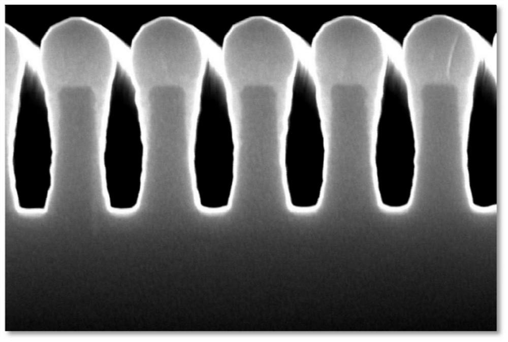
[0046](2) Using molecular beam epitaxial growth technique, a germanium intermediate layer having a periodic groove structure is epitaxially, which has a cyclical groove structure, and a growth temperature of 340 ° C, which is a germanium (113) crystal surface, and has a sawtooth. A pattern structure;
[0047] (3) Direct epitaxial growt...
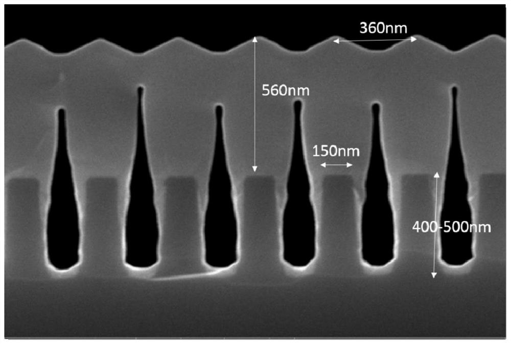
PUM
| Property | Measurement | Unit |
|---|---|---|
| depth | aaaaa | aaaaa |
| width | aaaaa | aaaaa |
| depth | aaaaa | aaaaa |
Abstract
Description
Claims
Application Information