LED transfer method and preparation method of LED display panel

A transfer method and display panel technology, which is applied in semiconductor/solid-state device manufacturing, electrical components, electric solid-state devices, etc., can solve problems such as technical difficulties and achieve high accuracy

Active Publication Date: 2019-11-05
CENTURY DISPLAY (SHENZHEN) CO LTD
View PDF10 Cites 3 Cited by
  • Summary
  • Abstract
  • Description
  • Claims
  • Application Information

AI Technical Summary

Problems solved by technology

[0002] At present, the size of LEDs tends to be miniaturized more and more, which makes it technically difficult to transfer a large number of tiny LEDs to a receiving substrate.

Method used


Image

  • LED transfer method and preparation method of LED display panel
  • LED transfer method and preparation method of LED display panel
  • LED transfer method and preparation method of LED display panel

Examples


Embodiment Construction

[0028] An embodiment of the present invention provides a method for transferring a light emitting diode (Light Emitting Diode, LED), which is combined below Figure 1 to Figure 13 Each step of the LED transfer method is described in detail. The transfer method includes the following steps.

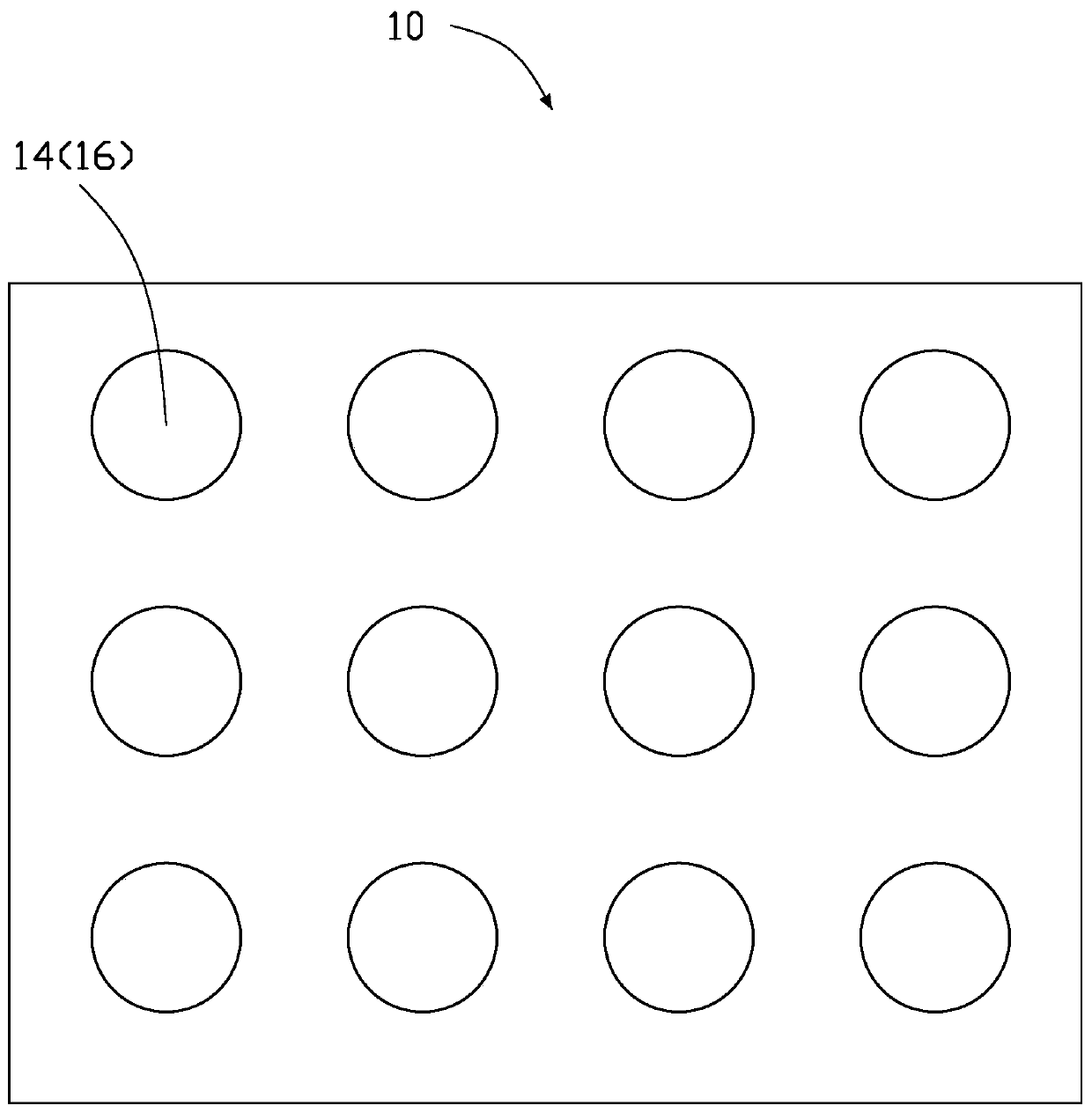
[0029] Step S11 : providing a receiving substrate 10 and a plurality of LEDs 20 .

[0030] Such as figure 1 As shown, the receiving substrate 10 has a plurality of receiving areas 14, and each receiving area 14 is used to receive one LED 20 correspondingly.

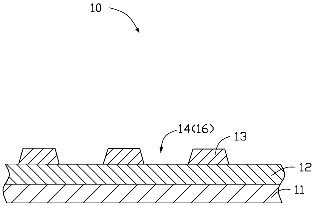
[0031] Such as figure 2 As shown, the receiving substrate 10 is a thin film transistor (Thin Film Transistor, TFT) substrate, which includes a substrate 11 , a TFT array layer 12 on the side of the substrate 11 , and an insulating layer 13 on the side of the TFT array layer 12 away from the substrate 11 . The TFT array layer 12 includes a plurality of TFTs (not shown), and the insulating layer 13 is provided with a plurality of r...


PUM


Abstract

An LED transferring method comprises the following steps: providing a receiving substrate and a plurality of LEDs, wherein the receiving substrate is provided with a plurality of receiving areas, eachreceiving area is used for correspondingly receiving one LED, and the two opposite ends of each LED are provided with a first electrode and a second electrode which are opposite in magnetism or magnetic attraction materials respectively; magnetically adsorbing a plurality of LEDs by using the first electromagnetic flat plate, so that each LED is transferred to a first platform after keeping a first electrode upward or a second electrode upward; magnetically adsorbing a plurality of LEDs on the first platform by using a second electromagnetic flat plate, and transferring the LEDs to a second platform after coarse positioning; and adsorbing the plurality of LEDs on the second platform by using a third electromagnetic flat plate, so that the LEDs are correspondingly transferred to the receiving area of the receiving substrate after being finely positioned. The invention further provides a preparation method of an LED display panel.

Description

technical field [0001] The invention relates to the field of display technology, in particular to a method for transferring a light emitting diode (Light Emitting Diode, LED) and a method for preparing an LED display panel. Background technique [0002] At present, the size of LEDs tends to be miniaturized more and more, which makes it technically difficult to transfer a large number of tiny LEDs to a receiving substrate. Contents of the invention [0003] The invention provides a method for transferring an LED, which comprises the following steps: [0004] Step S11: provide a receiving substrate and a plurality of LEDs, the receiving substrate has a plurality of receiving areas, each receiving area is used to receive one of the LEDs, and the opposite ends of each LED are respectively provided with magnetically opposite first an electrode and a second electrode or material available for magnetic attraction; [0005] Step S12: providing a first electromagnetic plate, usin...

Claims


Application Information

Patent Timeline
Patent Type & Authority Applications(China)
IPC IPC(8): H01L21/67H01L21/683H01L27/15H01L33/48
CPCH01L27/156H01L21/67144H01L21/683H01L33/48H01L2933/0033H01L21/67709H01L25/0753H01L33/0095H01L24/95H01L2924/12041H01L24/75H01L2224/75735H01L2224/95133H01L2924/15153
Inventor 林永富陈柏良
Owner CENTURY DISPLAY (SHENZHEN) CO LTD
Why Eureka
Try Eureka