

Light-emitting diode chip array and display panel
A technology of light-emitting diodes and chip arrays, which is applied to electrical components, electric solid devices, circuits, etc., can solve the problems of short-circuiting of adjacent LED chip electrodes and small display pixels, and achieve simple structure, increased area, and improved yield. Effect
- Summary
- Abstract
- Description
- Claims
- Application Information
AI Technical Summary
Problems solved by technology
Method used
Image

Examples
Embodiment Construction
[0033] The present invention will be further described in detail below in conjunction with the accompanying drawings and embodiments. It should be understood that the specific embodiments described here are only used to explain the present invention, but not to limit the present invention. In addition, it should be noted that, for the convenience of description, only some structures related to the present invention are shown in the drawings but not all structures.
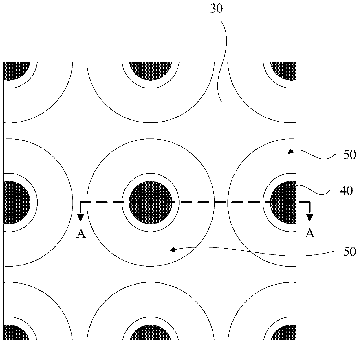
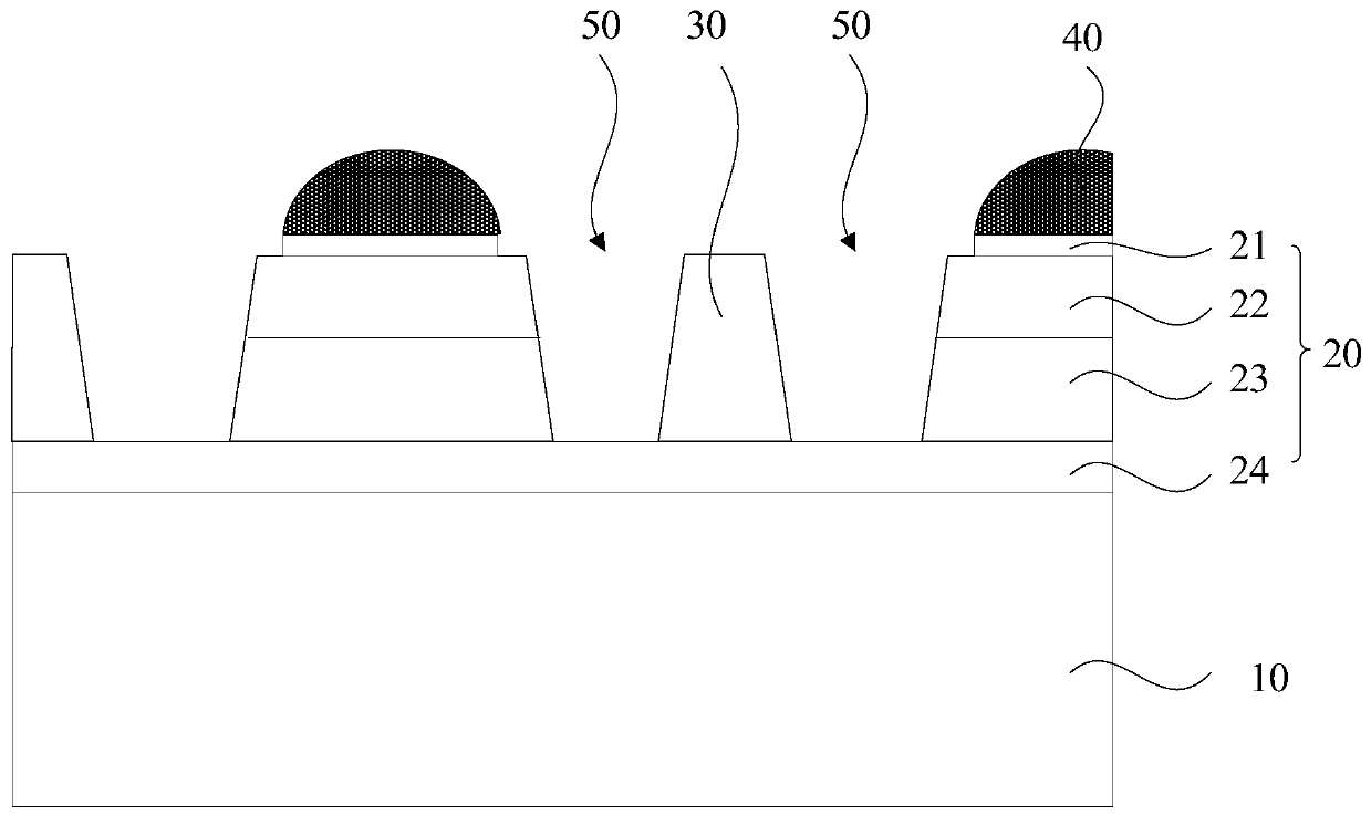
[0034] figure 1 It is a schematic top view structural diagram of a light emitting diode chip array provided by an embodiment of the present invention, figure 2 for along figure 1 Schematic diagram of the cross-sectional structure of A-A. see figure 1 and figure 2 , the light emitting diode chip array includes: a substrate 10 , a plurality of light emitting diode chips 20 , isolation walls 30 and solder joints 40 . A plurality of LED chips 20 and isolation walls 30 are located on the substrate 10 , and the L...
PUM
 Abstract
Description
Claims
Application Information