Touch display device
A touch display device, touch panel technology, applied in the direction of electronic equipment, applications, coatings, etc., can solve the problem that the display device affects the visual effect, and achieve the effect of improving the rainbow pattern phenomenon and improving the visual effect
- Summary
- Abstract
- Description
- Claims
- Application Information
AI Technical Summary
Problems solved by technology
Method used
Image
Examples
Embodiment 1
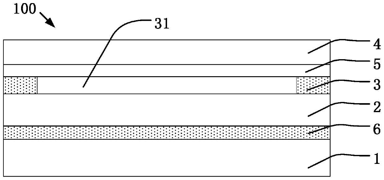
[0029] like figure 1 As shown, this embodiment provides a touch display device 100 , including a display panel 1 , a touch panel 2 , a first adhesive layer 3 , a cover plate 4 and a microstructure layer 5 .
[0030] The display panel 1 is a liquid crystal display panel, an organic light-emitting diode display panel, an active matrix organic light-emitting diode display panel, or a polymer light-emitting diode display panel.
[0031] The touch panel 2 is arranged on the upper surface of the display panel 1; the shape and size of the touch panel 2 are the same as those of the display panel 1, thereby effectively ensuring that the touch panel 2 The operable area of is consistent with the operable area of the display panel 1 .
[0032] The first adhesive layer 3 is ring-shaped and arranged at the edge of the upper surface of the touch panel 2; the middle part of the first adhesive layer 3 is surrounded to form a vacuum chamber 31; specifically, the first adhesive layer 3 Set...
Embodiment 2
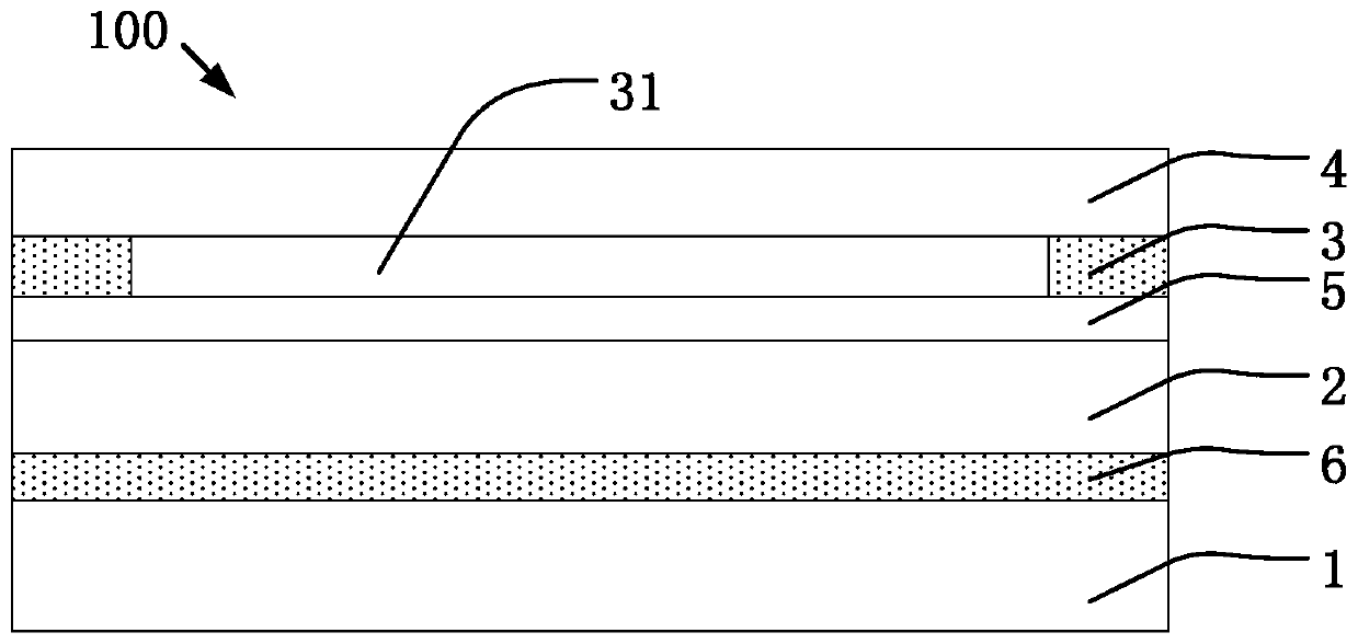
[0043] like image 3 As shown, the second embodiment includes all the technical features of the first embodiment, the difference is that the microstructure layer 5 in the second embodiment is arranged on the touch panel 2 facing the cover plate 4 One side surface, instead of the microstructure layer 5 in the first embodiment, is disposed on the surface of the cover plate 4 facing the touch panel 2 . The microstructure layer 5 can effectively improve reflection visual interference.
[0044] like figure 2 As shown, the microstructure layer 5 includes the antiglare film 51 and the base layer 52 ; the antiglare film 51 is disposed on the base layer 52 . The presence of the base layer 52 enables the microstructure layer 5 to be attached to the touch panel 2 through the base layer 52 instead of just being formed on the touch panel 2 through atomization. The microstructure layer 5 . This is convenient and saves process time.
Embodiment 3
[0046] like Figure 4a , Figure 4b As shown, in order to further enhance the display effect, all the technical features in the first embodiment and the second embodiment are included in the third embodiment, the difference is that the third embodiment can also be separated from the cover plate 4 A layer of the microstructure layer 5 is provided on the surface of one side of the touch panel 2 .
[0047] like Figure 4a , Figure 4b Shown are two structural schematic diagrams in the third embodiment, and the difference is that Figure 4a The microstructure layer 5 is provided on the surface of the cover plate 4 facing the touch panel 2; Figure 4b The microstructure layer 5 is disposed on the surface of the touch panel 2 facing the cover plate 4 .
[0048] It is worth noting that, if Figure 4a , Figure 4b As shown, the microstructure layer 5 can be above and below the cover plate 4 at the same time. By setting two microstructure layers 5 above and below the cover plate...
PUM
| Property | Measurement | Unit |
|---|---|---|
| haze | aaaaa | aaaaa |
Abstract
Description
Claims
Application Information
 - R&D
- Intellectual Property
- Life Sciences
- Materials
- Tech Scout
- Unparalleled Data Quality
- Higher Quality Content
- 60% Fewer Hallucinations
Browse by: Latest US Patents, China's latest patents, Technical Efficacy Thesaurus, Application Domain, Technology Topic, Popular Technical Reports.
© 2025 PatSnap. All rights reserved.Legal|Privacy policy|Modern Slavery Act Transparency Statement|Sitemap|About US| Contact US: help@patsnap.com


