Display panel and display panel manufacturing method

A display panel and plane technology, applied in the direction of instruments, identification devices, etc., can solve the problem of non-uniformity of the metal wiring area between the stress neutral layer and the driving circuit layer, and achieve the effect of alleviating stress concentration

Inactive Publication Date: 2019-11-08
WUHAN CHINA STAR OPTOELECTRONICS SEMICON DISPLAY TECH CO LTD
View PDF7 Cites 14 Cited by
  • Summary
  • Abstract
  • Description
  • Claims
  • Application Information

AI Technical Summary

Problems solved by technology

[0005] The present invention provides a display panel and a preparation method of the display panel, so as to alleviate the technical problem that the stress neutral layer in the bending area of ​​the existing display panel is not uniform with the metal wiring area of ​​the driving circuit layer

Method used


Image

  • Display panel and display panel manufacturing method
  • Display panel and display panel manufacturing method
  • Display panel and display panel manufacturing method

Examples


Embodiment Construction

[0041] The following descriptions of the various embodiments refer to the accompanying drawings to illustrate specific embodiments in which the invention may be practiced. The directional terms mentioned in the present invention, such as [up], [down], [front], [rear], [left], [right], [inner], [outer], [side], etc., are only for reference Additional schema orientation. Therefore, the directional terms used are for describing and understanding the present invention, not for limiting the present invention. In the figures, units with similar structures are denoted by the same reference numerals.

[0042] The present invention provides a display panel and a manufacturing method of the display panel, so as to alleviate the technical problem that the stress neutral layer in the bending area and the metal wiring area of ​​the driving circuit layer are not unified in the existing display panel.

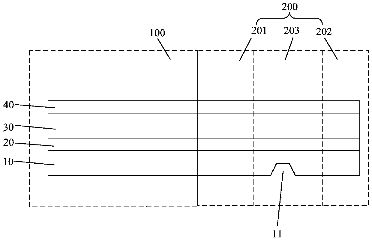
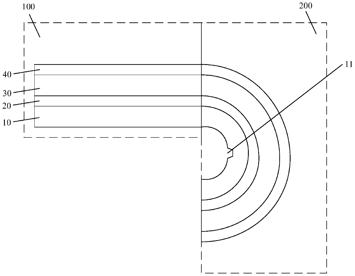
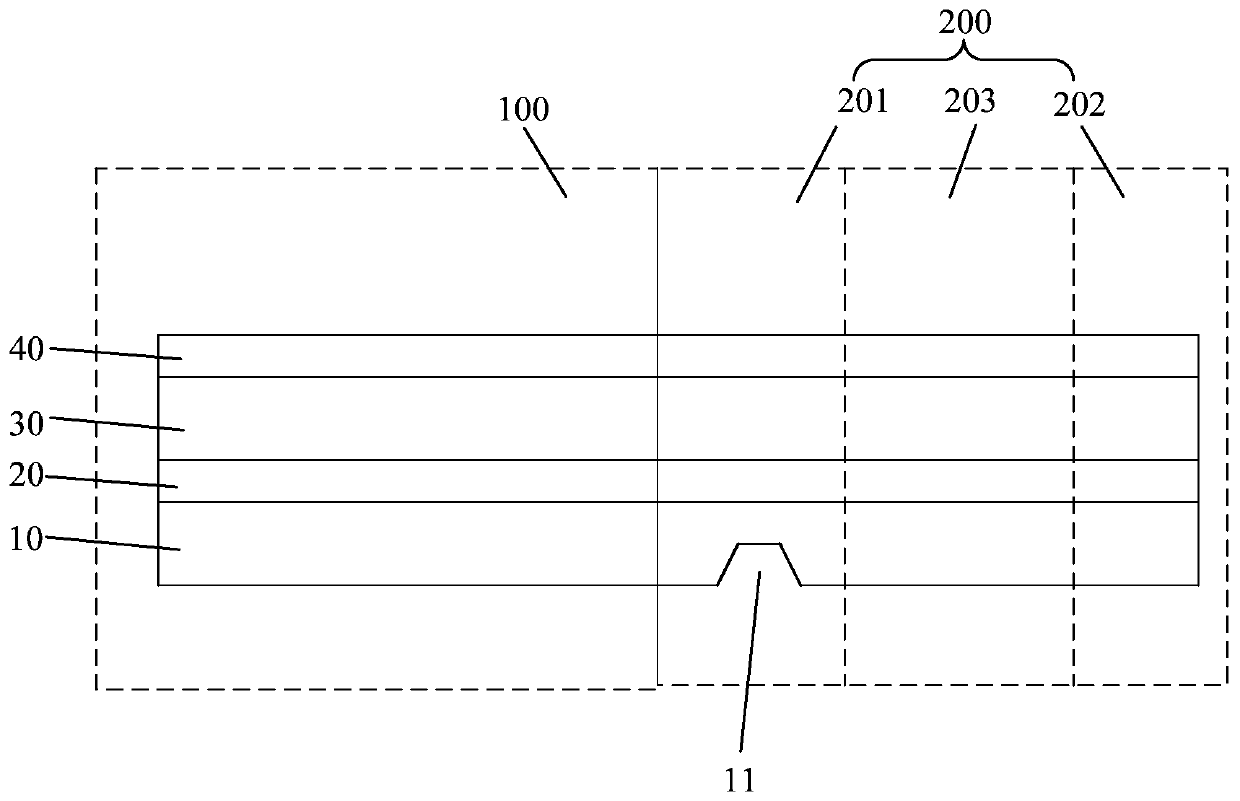
[0043] like figure 1 As shown, it is a first structural schematic diagram of a display...


PUM


Abstract

The present invention provides a display panel and a display panel manufacturing method. The display panel comprises a planar area and a bending area connected with the planar area, and the display panel further comprises a flexible substrate and a driving circuit layer; the flexible substrate comprises at least a first flexible layer, a barrier layer formed on one side of the first flexible layerand a second flexible layer formed on the side, away from the first flexible layer, of the barrier layer; the driving circuit layer is formed on the side, away from the barrier layer, of the second flexible layer; and in the bending area, a groove is formed on the side, away from the barrier layer, of the first flexible layer. According to the technical scheme of the present invention, by settingthe groove in the first flexible layer in the bending area, the thickness of the first flexible layer in the bending area can be reduced, and a stress neutral layer in the bending area can approach the metal trace area of the driving circuit layer, so that the technical problems of stress concentration and metal trace breakage in the bending area can be alleviated.

Description

technical field [0001] The present invention relates to the field of display technology, and in particular, to a display panel and a preparation method of the display panel. Background technique [0002] With the development of technology in the display industry, full-screen technology has become a major development trend. The design of bending the non-display area of ​​the display panel to the back of the display area is an important means to realize the narrow border of the display panel. [0003] Existing display panels usually need to use a flexible substrate to achieve the bending effect. However, after the flexible substrate is bent, the stress neutral layer and the metal wiring area of ​​the driving circuit layer are often inconsistent in the bending area, causing the bending The area is prone to stress concentration and metal wiring breakage. [0004] Therefore, the existing display panel has the technical problem that the stress neutral layer in the bending area is...

Claims


Application Information

Patent Timeline
IPC IPC(8): G09F9/30G09F9/33
CPCG09F9/301G09F9/33
Inventor 柯霖波梁博吴梦莹
Owner WUHAN CHINA STAR OPTOELECTRONICS SEMICON DISPLAY TECH CO LTD
Why Eureka
Try Eureka