Display panel and preparation method thereof
A display panel and substrate technology, applied in nonlinear optics, instruments, optics, etc., can solve the problems of product air bubbles, affecting the normal elastic range of PS film columns, affecting product yield, etc., and achieving the effect of improving air bubbles
- Summary
- Abstract
- Description
- Claims
- Application Information
AI Technical Summary
Problems solved by technology
Method used
Image
Examples
Embodiment Construction
[0027] The following descriptions of the various embodiments refer to the accompanying drawings to illustrate specific embodiments in which the invention may be practiced. The directional terms mentioned in the present invention, such as [top], [bottom], [front], [back], [left], [right], [inside], [outside], [side], etc., are only for reference The orientation of the attached schema. Therefore, the directional terms used are used to illustrate and understand the present invention, but not to limit the present invention. In the figures, structurally similar elements are denoted by the same reference numerals.
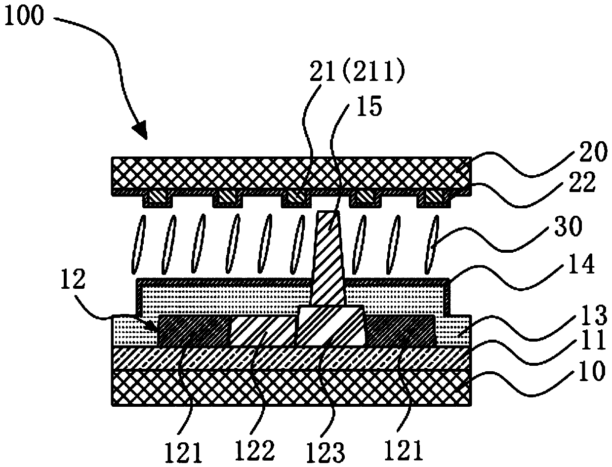
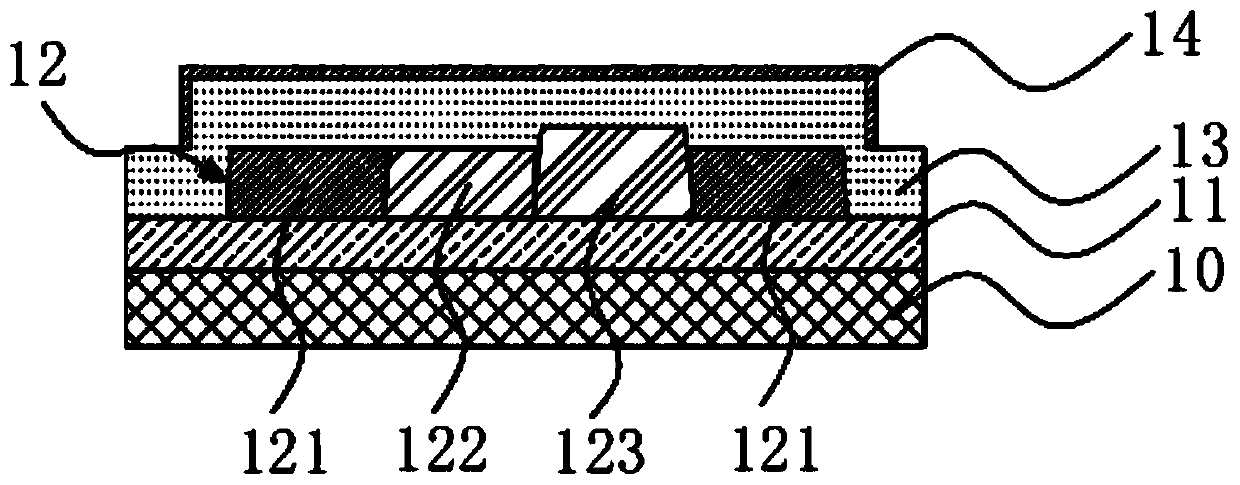
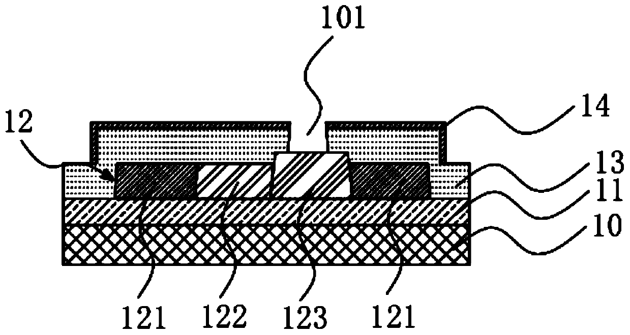
[0028] The present invention is aimed at the existing display panel. Since the PS film column is set on the PFA film layer, the PFA film layer collapses or rebounds under pressure, thereby affecting the normal elastic range of the PS film column on the upper layer, thereby causing the product to be under pressure. Bubbles appear in a high-altitude and low-pressure envi...
PUM
| Property | Measurement | Unit |
|---|---|---|
| thickness | aaaaa | aaaaa |
Abstract
Description
Claims
Application Information


