Display substrate and preparation method thereof and display device
A technology for display substrates and peripheral displays, which is used in semiconductor/solid-state device manufacturing, electrical components, and electrical solid-state devices, etc., and can solve problems such as poor film thickness uniformity
- Summary
- Abstract
- Description
- Claims
- Application Information
AI Technical Summary
Problems solved by technology
Method used
Image

Examples
no. 1 example
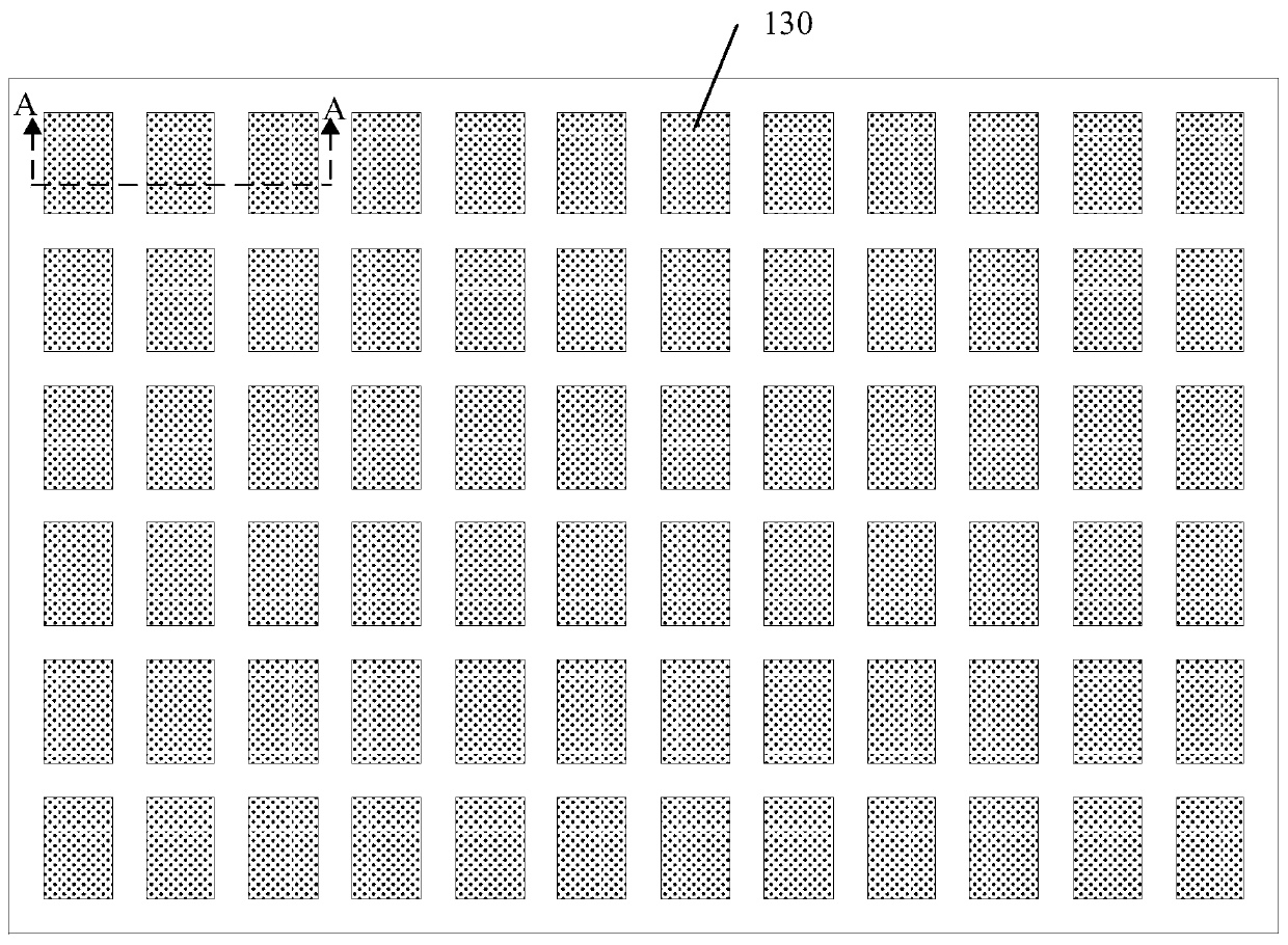
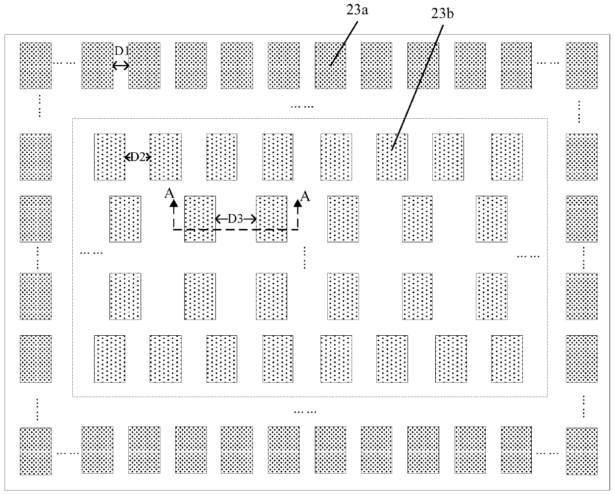
[0032] image 3 It is an example diagram of the display substrate of the first embodiment of the present application; Figure 4 for image 3 An example diagram of the cross-section in the direction of A-A. Such as image 3 and Figure 4 As shown, the display substrate provided in this embodiment includes: a peripheral display area ( image 3 The area outside the dotted line box) and the central display area ( image 3 area within the dashed box). Wherein, a plurality of first pixel units 23a are regularly arranged in the peripheral display area, and a plurality of second pixel units 23b are regularly arranged in the central display area.
[0033] In this embodiment, the pixel density of the first pixel unit 23a in the peripheral display area is greater than the pixel density of the second pixel unit 23b in the central display area. Such as image 3 As shown, the distance (eg, D1) between adjacent first pixel units 23a in the peripheral display area is smaller than the ...
no. 2 example
[0052] This embodiment is an extension of the aforementioned first embodiment. The main structure of the display substrate in this embodiment is basically the same as that of the aforementioned first embodiment. The difference is that the area of the first pixel unit 23a in the peripheral display area is larger than that Areas of the second pixel units (for example, the second pixel units 23b and 23c) within the region.
[0053] Such as Figure 6 and Figure 7As shown, in this embodiment, the area of the first pixel unit 23a in the peripheral display area is larger than that of the second pixel unit in the central display area, and the distance between adjacent first pixel units 23a in the peripheral display area (such as , D1) is less than the distance between adjacent second pixel units in the central display area (for example, D2 or D3), so that the pixel density of the first pixel unit in the peripheral display area is greater than that of the second pixel unit in the...
no. 3 example
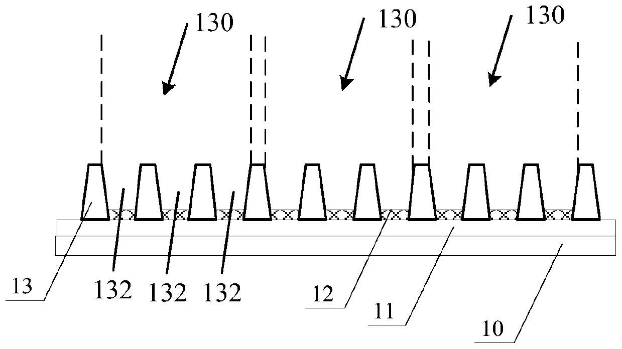
[0058] Figure 8 It is an example diagram of the display substrate of the third embodiment of the present application; Figure 9 for Figure 8 An example diagram of the cross-section in the direction of A-A. Such as Figure 8 and Figure 9 As shown, the display substrate provided in this embodiment includes: a peripheral display area ( Figure 8 The area outside the dotted line box) and the central display area ( Figure 8 area within the dashed box). Wherein, a plurality of first pixel units 23a are regularly arranged in the peripheral display area, and a plurality of second pixel units 23b and second pixel units 23c are regularly arranged in the central display area. Wherein, the area of the first pixel unit is larger than the area of the second pixel unit, and the pixel density in the peripheral display area is equal to the pixel density in the central display area.
[0059] Such as Figure 9 As shown, the display substrate includes a substrate 20, a driving str...
PUM
 Abstract
Description
Claims
Application Information
 - R&D
- Intellectual Property
- Life Sciences
- Materials
- Tech Scout
- Unparalleled Data Quality
- Higher Quality Content
- 60% Fewer Hallucinations
Browse by: Latest US Patents, China's latest patents, Technical Efficacy Thesaurus, Application Domain, Technology Topic, Popular Technical Reports.
© 2025 PatSnap. All rights reserved.Legal|Privacy policy|Modern Slavery Act Transparency Statement|Sitemap|About US| Contact US: help@patsnap.com