FLASH chip with independent BOOT area, system and method

A technology of chips and implementation methods, applied in the field of improvement of FLASH chips, systems and methods, capable of solving problems such as crashes, complex software, and unsmooth startup, and achieving the effect of realization preparation

Pending Publication Date: 2019-12-20
GENEW TECH
View PDF4 Cites 0 Cited by
  • Summary
  • Abstract
  • Description
  • Claims
  • Application Information

AI Technical Summary

Problems solved by technology

[0005] However, there are certain defects in the above two commonly used methods. The first kind of hardware design is complicated, and chip selection needs to be switched. At the same time, the hardware cost is increased because an additional BOOT FLASH needs to be soldered.
The second method is that the software is too complicated, and two sets of BOOT programs need to be maintained. There are many nested BOOT programs at different levels, and the startup process is also very complicated, which often causes problems such as unsmooth startup or even crashes.

Method used


Image

  • FLASH chip with independent BOOT area, system and method
  • FLASH chip with independent BOOT area, system and method
  • FLASH chip with independent BOOT area, system and method

Examples


Embodiment Construction

[0024] The following will provide a more detailed description of the preferred embodiments of the present invention in conjunction with the accompanying drawings.

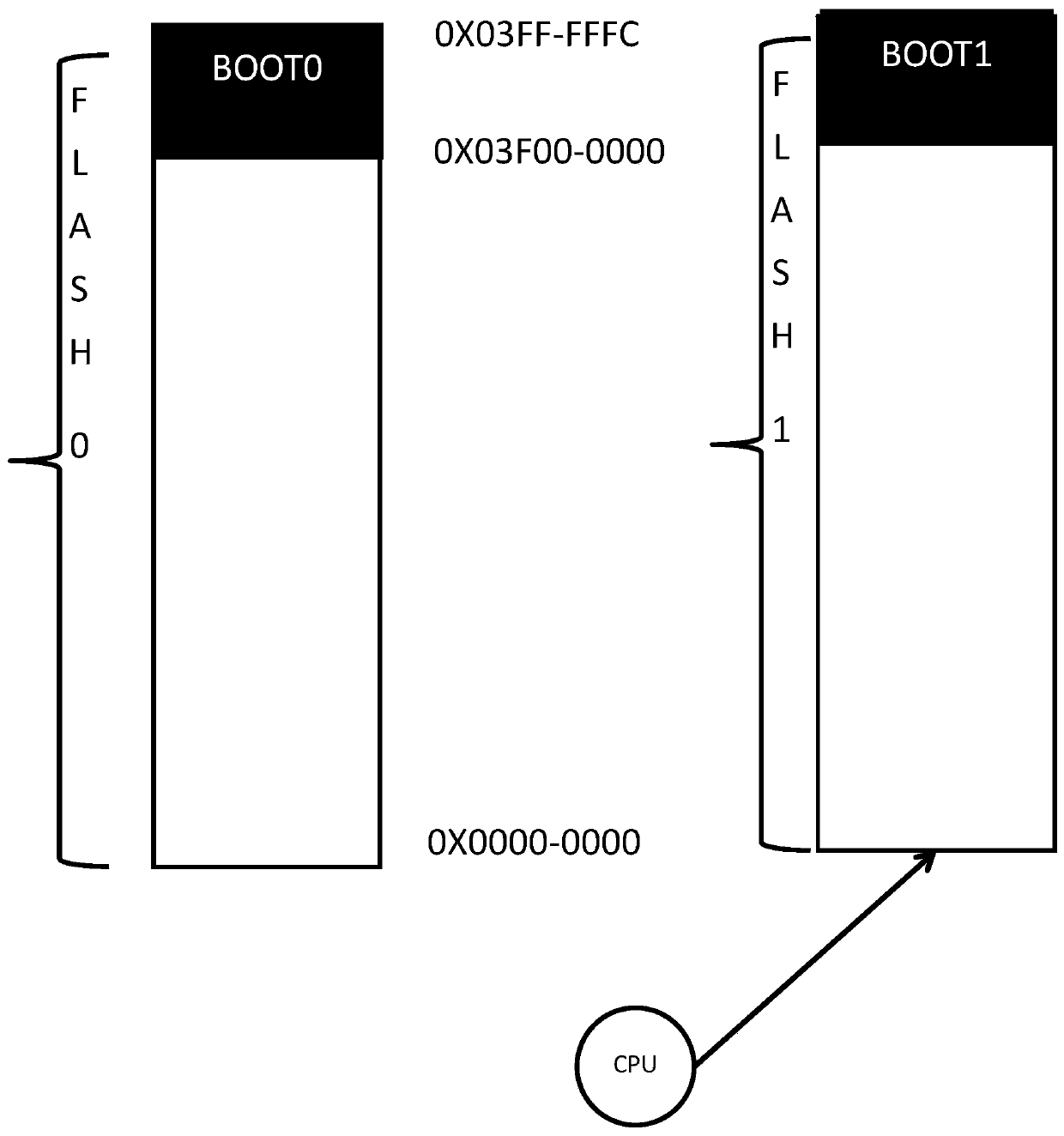
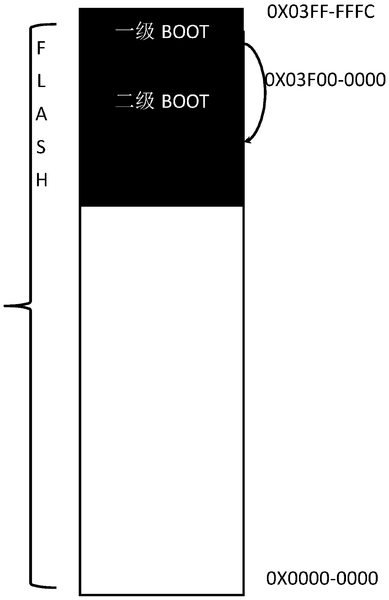
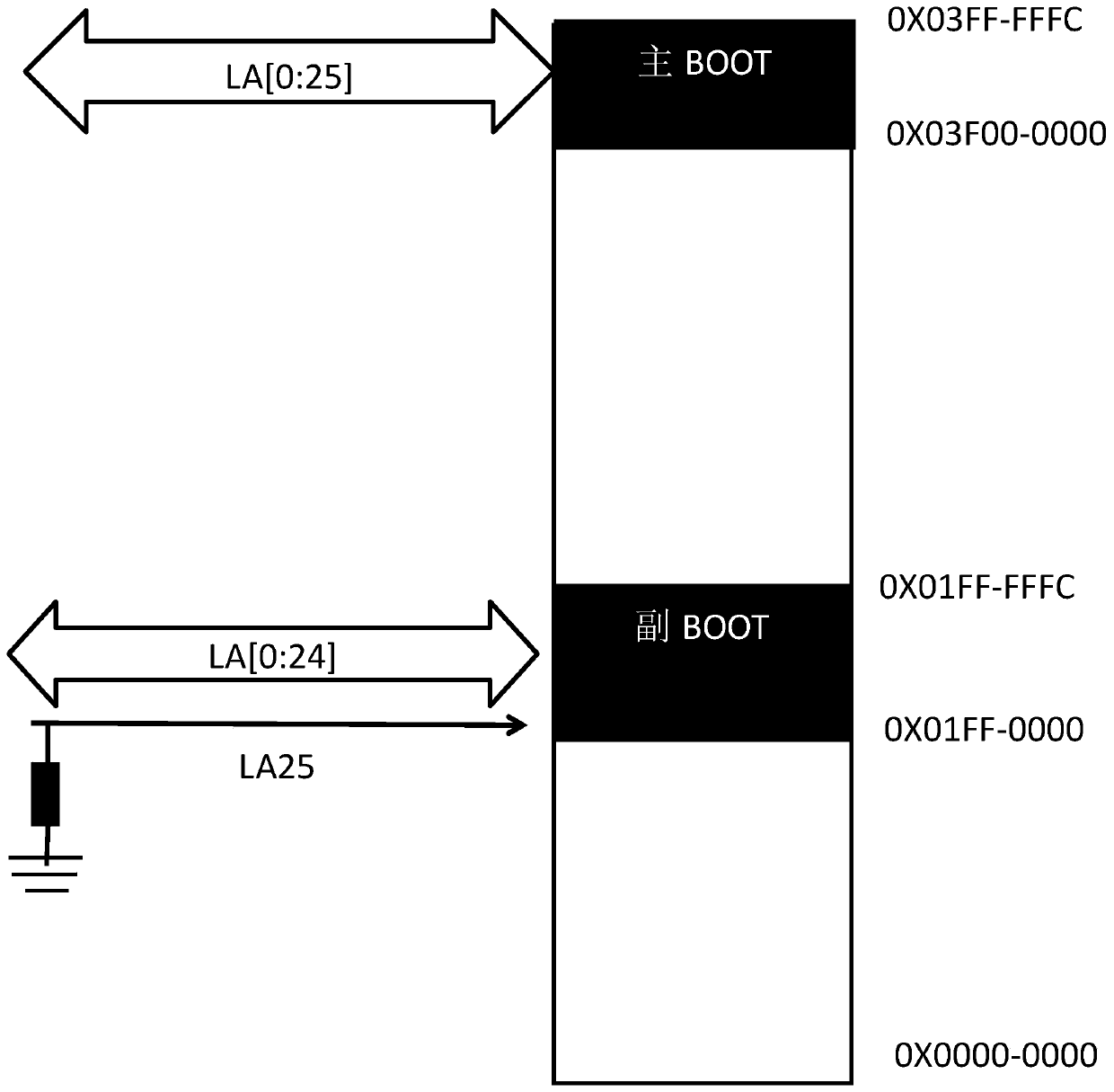
[0025] A kind of FLASH chip and system and method of setting independent BOOT area provided by the present invention, wherein said FLASH chip setting adopts described BOOT area to be set to be at least two, when being set to two, be set to have primary and secondary BOOT area , when there are more settings, there is a startup retrieval sequence. Sequentially set the start waiting time in each BOOT area, starting from the main boot area, after exceeding the start waiting time, jump to the next BOOT area to start, and wait in turn, if all BOOT areas cannot start If it is set to startup failure, it will display or prompt the information of startup failure.

[0026] The present invention takes PowerPC P1021 chip as example, the high-performance RICS (Reduced Instruction Set Computer, reduced instruction set computer) ...


PUM


Abstract

Provided is a FLASH chip with independent BOOT areas, system and method. In the chip, the BOOT areas are set as a main BOOT area and an auxiliary BOOT area and are sequentially set in the starting waiting preset time of the main BOOT area, and the FLASH chip is used for skipping to the auxiliary BOOT area to be started when the starting waiting preset time is exceeded. Due to the fact that the twoor more independent BOOT program areas are arranged in the FLASH chip, and a BOOT program area is arranged in one BOOT program area and enters the other BOOT program area to be started when the BOOTprogram area cannot be started after waiting for the preset time, preparation of multiple starting program areas is achieved.

Description

technical field [0001] The present invention relates to an embedded chip, a system and a method, and in particular to an improvement of a FLASH chip with an independent BOOT area, a system and a method. Background technique [0002] In the field of embedded systems, any CPU needs BOOT program to start. Such as figure 1 and figure 2 As shown, developers generally put the BOOT program in FLASH, but if the BOOT program is damaged, the board may not start at all, and the corresponding device cannot start to work at this time, and the corresponding device such as a mobile phone becomes a brick. . It can be seen that the upgrade and perfection of the BOOT program requires sufficient reliability and stability. [0003] In order to prevent the damage of the BOOT program from causing the mobile phone to become a brick, the common practice in the industry is to solder two pieces of FLASH on the single board and connect them to different chip selection signals of the CPU respecti...

Claims


Application Information

Patent Timeline
IPC IPC(8): G06F11/20G06F9/4401
CPCG06F11/2028G06F9/4403G06F9/4411
Inventor 李小军吴闽华孟庆晓
Owner GENEW TECH
Why Eureka
Try Eureka