

Method for realizing positioning of ZnO nanowire to field effect transistor substrate
A positioning method and nanowire technology, which is applied in the manufacture of electrical components, circuits, semiconductors/solid-state devices, etc., can solve problems such as inability to accurately locate and achieve layout registration, and achieve the effect of saving production costs
- Summary
- Abstract
- Description
- Claims
- Application Information
AI Technical Summary
Problems solved by technology
Method used
Image

Examples
Embodiment Construction
[0037] In order to make the object, technical solution and advantages of the present invention clearer, the present invention will be described in further detail below in conjunction with specific embodiments and with reference to the accompanying drawings.
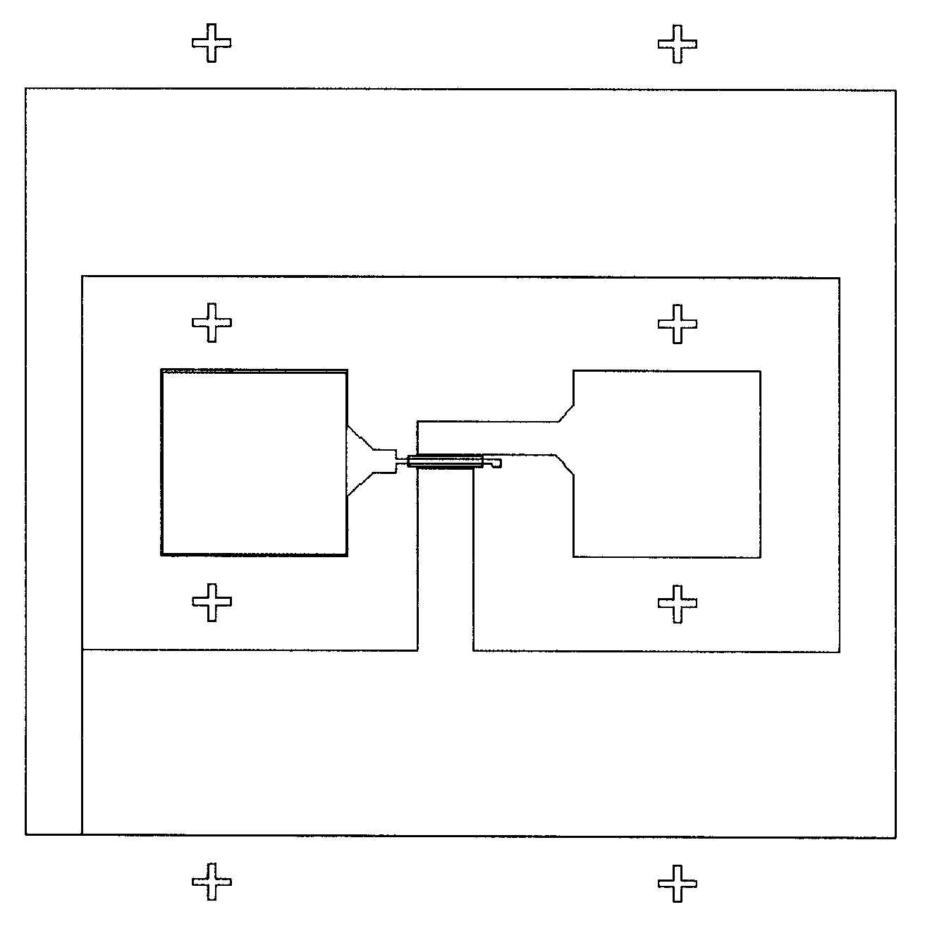
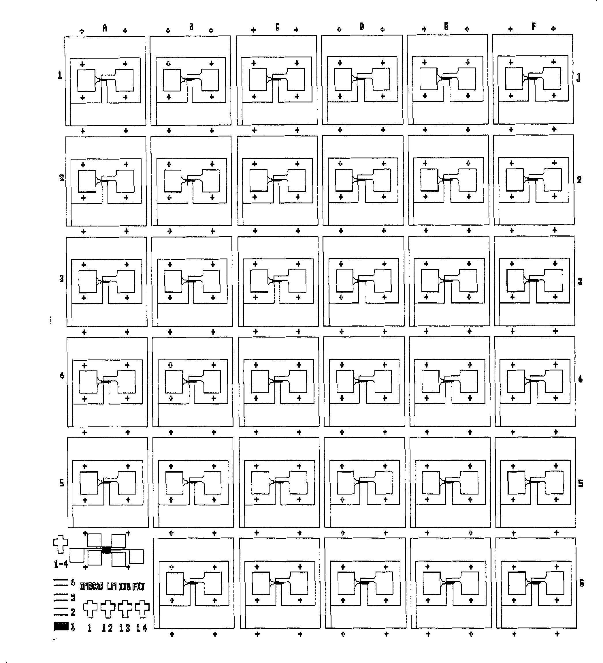
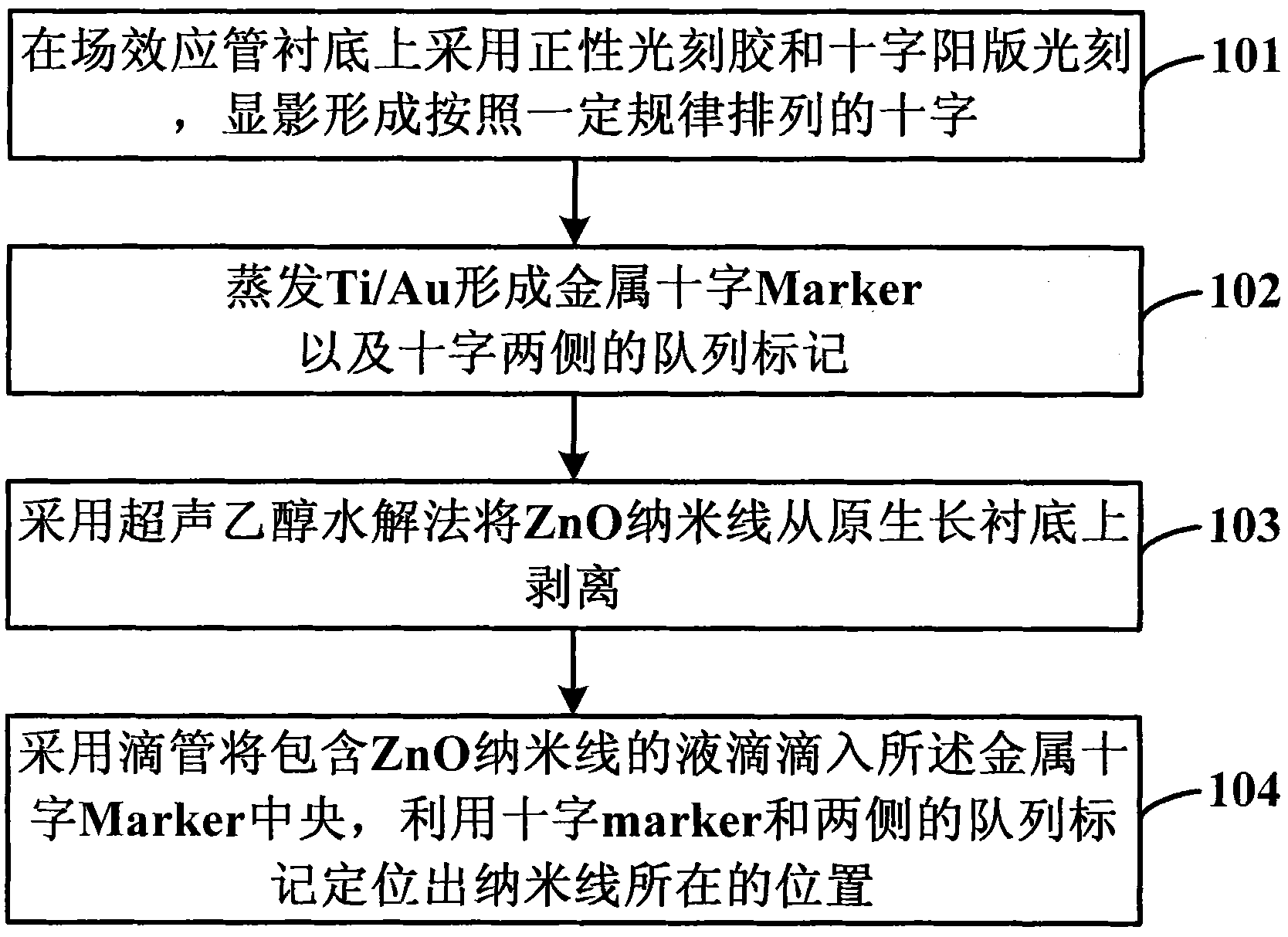
[0038] In the general ZnO nanowire field-effect transistor preparation process, it is necessary to peel off the ZnO nanowire from the self-growth substrate and deposit it on the P-type Si substrate. In the device preparation process, the ZnO nanowire must be accurately deposited on the substrate. For the fixed position on the bottom, we use photoetching a version of the cross mark on the P-type Si substrate, use 5214 reverse glue, reverse the positive plate photolithography to form a photoresist cross, and evaporate Ti (300 Angstroms) / Au ( 1000 Angstroms), forming metallic marks such as Figure 5 As shown in Fig. 1, the droplet rich in nanowires is dropped on the device substrate with a dropper, and the microscope is used...
PUM
| Property | Measurement | Unit |
|---|---|---|
| length | aaaaa | aaaaa |
| width | aaaaa | aaaaa |
| thickness | aaaaa | aaaaa |
Abstract
Description
Claims
Application Information