Method for realizing positioning of ZnO nanowire to field effect transistor substrate

A positioning method and nanowire technology, which are applied in the manufacturing of electrical components, circuits, semiconductor/solid-state devices, etc., can solve the problems of inability to accurately locate and achieve layout registration, and achieve the effect of saving production costs.

Inactive Publication Date: 2009-10-07
SEMICON MFG INT (SHANGHAI) CORP +1
View PDF0 Cites 0 Cited by
  • Summary
  • Abstract
  • Description
  • Claims
  • Application Information

AI Technical Summary

Problems solved by technology

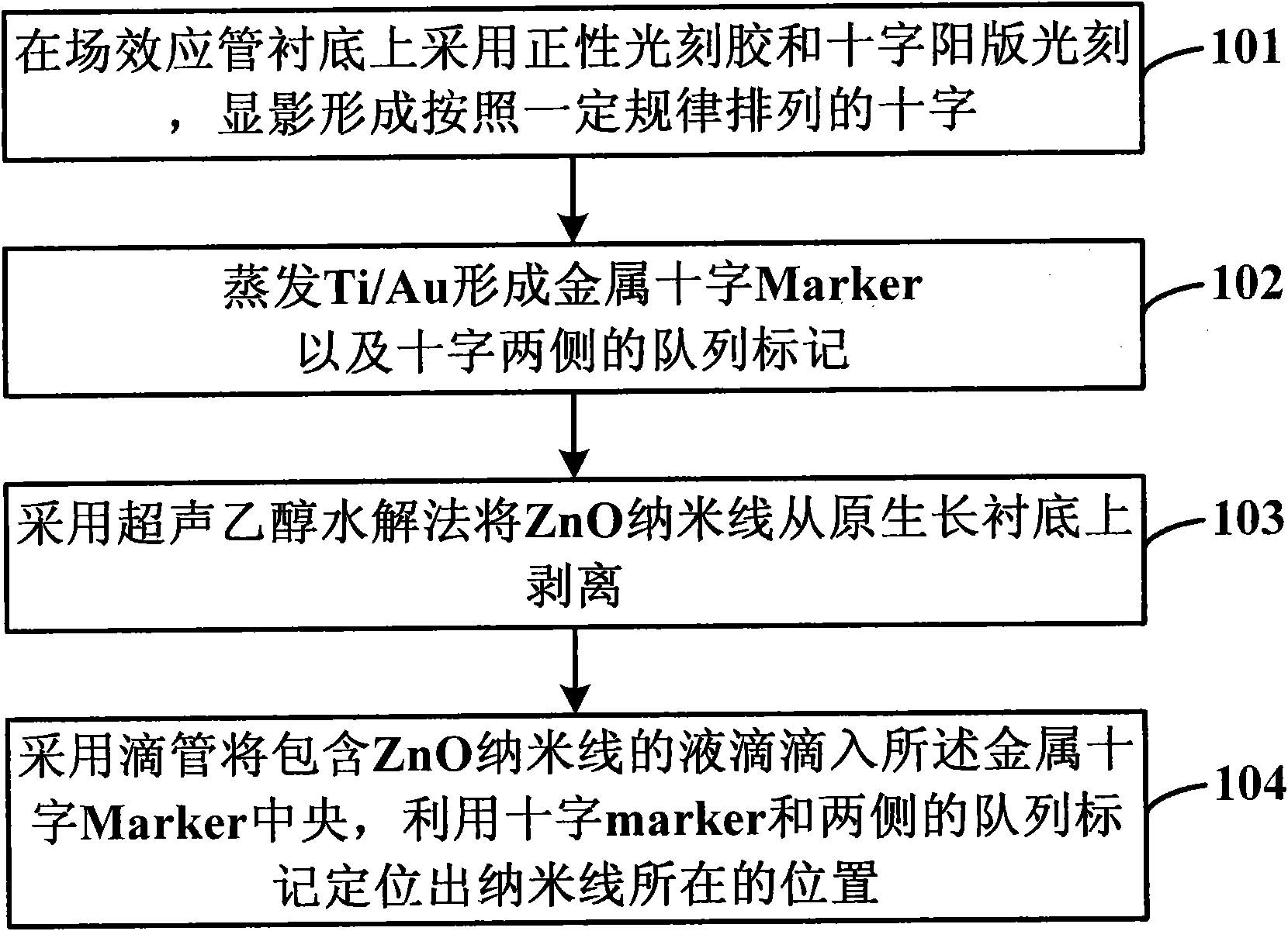
[0008] In view of this, the main purpose of the present invention is to provide a method for positioning the ZnO nanowires to the field effect transistor substrate, so as to solve the problem that the nanowires cannot be accurately positioned after being deposited on the P-type Si sheet substrate, so that subsequent field effect transistors cannot be realized. The layout registration problem in the preparation ensures that the source and drain metal can form ohmic contact with the ZnO nanowire channel

Method used


Image

  • Method for realizing positioning of ZnO nanowire to field effect transistor substrate
  • Method for realizing positioning of ZnO nanowire to field effect transistor substrate
  • Method for realizing positioning of ZnO nanowire to field effect transistor substrate

Examples


Embodiment Construction

[0037] In order to make the object, technical solution and advantages of the present invention clearer, the present invention will be described in further detail below in conjunction with specific embodiments and with reference to the accompanying drawings.

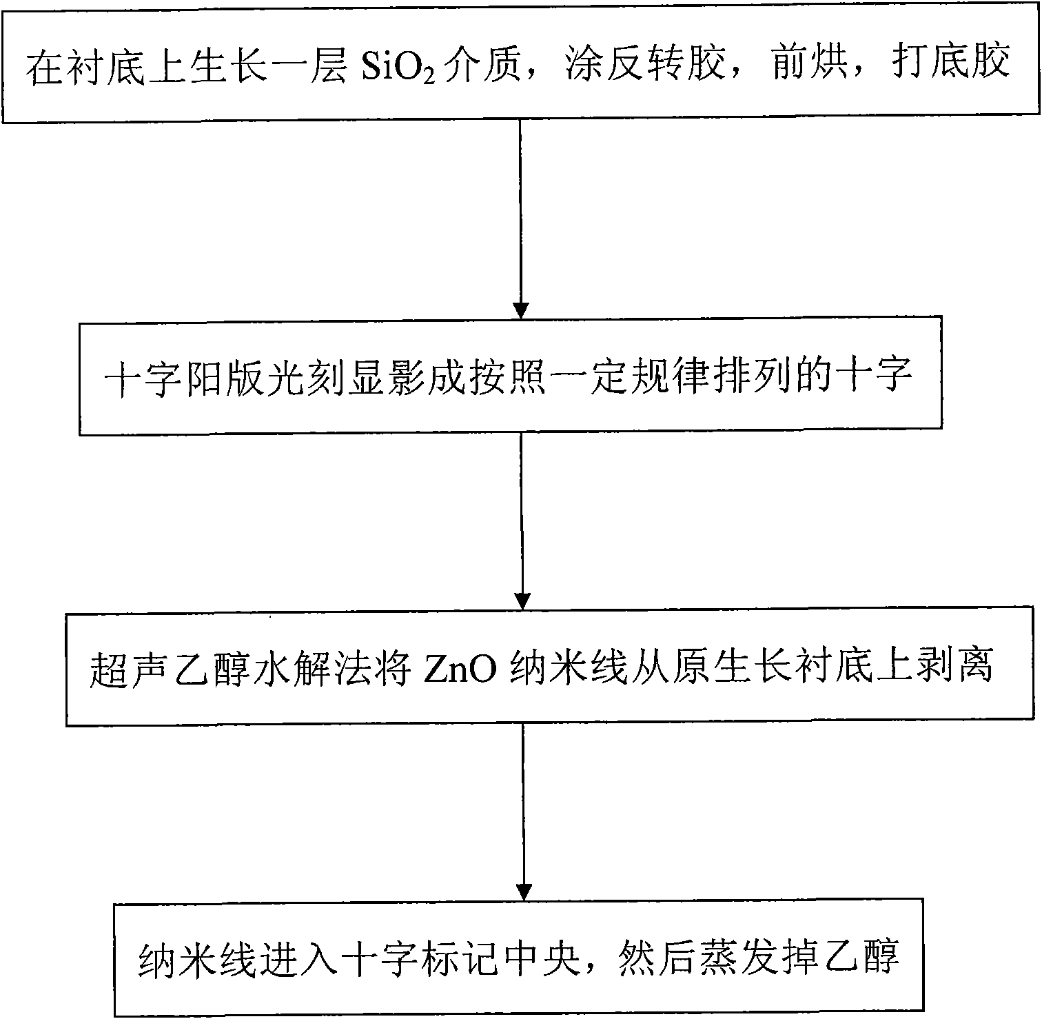
[0038] In the general ZnO nanowire field-effect transistor preparation process, it is necessary to peel off the ZnO nanowire from the self-growth substrate and deposit it on the P-type Si substrate. In the device preparation process, the ZnO nanowire must be accurately deposited on the substrate. For the fixed position on the bottom, we use photolithography of a cross mark on the P-type Si substrate, use 5214 reverse glue, reverse the positive plate photolithography to form a photoresist cross, evaporate Ti(300A) / Au(1000A ), form a metal Marker, such as Figure 5 As shown in Fig. 1, the droplet rich in nanowires is dropped on the device substrate with a dropper, and the microscope is used to observe repeatedly until the n...


PUM


Abstract

The invention discloses a method for realizing positioning of a ZnO nanowire to a field effect transistor substrate. The method comprises the following steps: positive photoresist and cross positive photoresist are adopted on the field effect transistor substrate, and regularly arranged crosses are formed by developing; the Ti / Au is vaporized to form a metal cross Marker and queue markers on both sides of the cross; the ZnO nanowire is stripped off from the original growth substrate by an ultrasonic ethanol hydrolysis method; and the liquid drop containing the ZnO nanowire is dropped to the center of the metal cross Marker through a dropper, and the position of the nanowire is positioned by using the metal cross Marker and the queue markers on both sides of the cross. By using the invention, the deposition and the positioning of the ZnO nanowire from the original glass substrate to the field effect transistor substrate are realized, the problem of random arrangement of the ZnO nanowire deposited on the device substrate is solved, and the accurate positioning of the ZnO nanowire is realized.

Description

technical field [0001] The invention relates to the technical field of compound semiconductor devices, in particular to a method for realizing the positioning of ZnO nanowires to a field effect tube substrate by using a cross marker. Background technique [0002] Nanowires (including nanotubes) are one of the most advanced topics in nanotechnology and condensed matter physics research. They have superior physical properties and are the structural units for constructing nanoscale components such as lasers, sensors, field-effect transistors, light-emitting diodes, logic circuits, spintronic devices, and quantum computers. [0003] Especially semiconductor nanowires, which can not only be used as basic building blocks, but also be used to connect various nanodevices. Through in-depth research on semiconductor nanowires, it is expected to prepare electronic, photon and spin information processing devices with complex functions on a single nanowire. [0004] In addition, a vari...

Claims


Application Information

Patent Timeline
Patent Type & Authority Applications(China)
IPC IPC(8): H01L21/335H01L21/368
Inventor 黎明张海英付晓君徐静波
Owner SEMICON MFG INT (SHANGHAI) CORP
Why Eureka
Try Eureka